In a fast-changing world where product development cycles are becoming compressed into months rather than years, a company whose chips can be programmed and reprogrammed on the fly would appear to have a natural advantage. Enter Xilinx, the San Jose, California-headquartered developer of FGPAs. The F in FPGA stands for field, as in field-programmable gate array, but it could so easily stand for fast, flexible or future-proof – all of which are qualities that these devices possess.
Founder Ross Freeman is credited with inventing the FPGA more than 30 years ago. He realised that, owing to Moore's Law, transistors would be getting less expensive and more powerful each year, making customisable programmable chips affordable. But Zilog, where he worked at the time, wouldn’t fund his idea, so he left to set up his own company, along with colleagues James V Barnett II and Bernard Vonderschmitt.
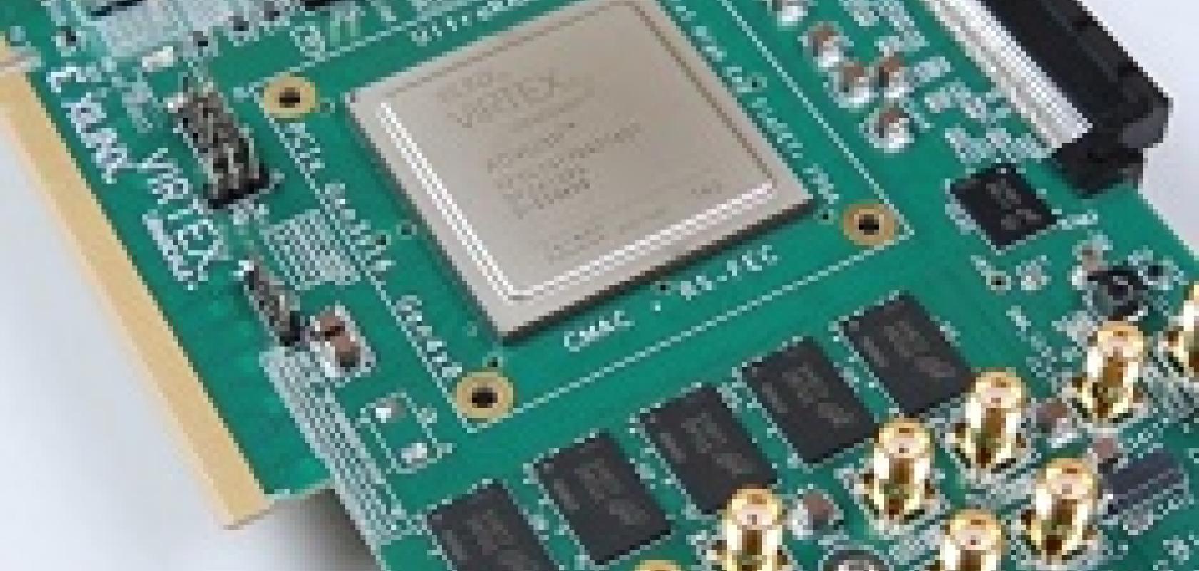
Fast forward to the present, and transistor technology has developed to the point that it would probably be unrecognisable to Freeman. Last year, Xilinx started shipping some of the most advanced integrated circuits on the market, its UltraScale+ devices made in 16nm FinFET silicon process technology from TSMC. One of the new Xilinx 16nm FPGAs packs in 5.2 billion transistors, another one supports seven programmable cores.
 ‘Technology is absolutely critical to success, particularly in the wider communications market,’ stated Giles Peckham, regional marketing director at Xilinx. Offering the latest technology wins over the customers who are trying to be on the leading edge of technology and systems themselves, he says. And that’s one of the key reasons that the company has grown its market share substantially over the last five years.
‘If we go back to fiscal year 2011, which is typically calendar 2010, we had about 53 per cent market share in what we call the programmable logic market,’ said Peckham. ‘We switched foundries to TSMC for 28nm and discovered pretty rapidly that TSMC is the best manufacturing partner in the world for technology.’
He continued: ‘Xilinx developed a range of products on TSMC’s 28nm technology, and by working very closely together with our communications customers the company developed architectures and products that were much more suited to their needs. That gave us greater market share at that node than we had had at the previous node.’
Based on that experience, Xilinx moved onto the 20nm node, primarily for the communications market. When moving on to the higher nodes at 20nm and then 16nm, Xilinx was at least one year ahead of its competitors, such that it is currently the only FPGA provider offering products at the 16nm node. And the next node is on the horizon. Xilinx plans to skip 10nm and move straight to 7nm FinFET, when TSMC starts up its new production line in 2017.
In addressing the market, technology itself is not enough, Peckham adds. ‘We have to address the system level needs of our customers,’ he said. ‘We have really migrated during that time from our early days when we called ourselves the programmable logic company, we are now what we call the all programmable solutions provider for many diverse markets.’
In order for its products to be adopted as widely as possible, Xilinx has been tearing down the barriers to programming its devices. ‘We’ve recognised that we need to extend the programming models that we use. When I started designing, we were using schematic capture and we’ve moved onto HDL – hardware description languages – and now moved onto describing what we want to implement in those devices at much higher levels: C++ and Open CL,’ Peckham explained.
All programmable
Xilinx is currently targeting four key market megatrends with its products: cloud computing, embedded vision, the industrial Internet of Things and 5G mobile. Out of those, the cloud computing segment is showing the fastest growth, according to Peckham. ‘We’ve identified three areas where we have a strong value proposition, and that’s storage, networking and compute,’ he said. ‘We believe there’s another $6 billion of business that we can address in those areas over the next five years.
An FPGA is a common part that can be programmed in many different ways to suit different applications. Yet, as the FPGA business has become more competitive and more diverse, Xilinx has started to make its FPGAs somewhat tailored to the end markets. (Here we will just talk about the cloud computing segment of its business).
The high-end all programmable devices, the Kintex and Virtex families built in the Ultrascale and Ultrascale+ architectures include high-speed input/output transceivers, a large number of digital signal processing (DSP) ‘slices’ and a variety of options for on-board memory. The 28Gb/s backplane transceiver capabilities of its UltraScale and UltraScale+ architecture make it possible to implement terabit systems. Within each product family, each platform contains a different ratio of features to address the needs of advanced logic designs; for example, some platforms are optimised for pure performance or bandwidth, while others are intended to give the right blend of system performance with the lowest cost or smallest power envelope.
In the past FPGAs were used for rapid prototyping before moving to an application specific integrated circuit (ASIC) or application-specific standard product (ASSP). Today, however, the FPGA is often the first choice for prototyping as well as for system production, because it allows companies to get their products to market much faster, and even to update their designs in the field as standards or their requirements evolve.
For customers who don’t have the expertise in-house to develop the product that they need, Xilinx has built up a strong intellectual property portfolio. While some customers – such as the hyperscale data centre operators – will develop their own solution and their own code for the FPGA, others will look for building blocks to do the integration themselves, while yet others will turn to Xilinx and say ‘Xilinx, can you help us?’ We want to use your IP and please do the integration for us.
Now, when you hear about the latest developments in communications chips, the chances are that Xilinx is leading the way. At OFC 2016 in Anaheim earlier this year, Xilinx had no fewer than four demonstrations, each a first of some kind.
The company showed the world's first implementation of Flexible Ethernet transport or FlexE. Recognising that router interfaces and optical transport were developing at different paces, the industry needed a method to match their capacities without wasting valuable bandwidth. So the Optical Internetworking Forum (OIF), backed by companies including Google and Facebook, fast-tracked an implementation agreement that specifies ways to support Ethernet MAC rates that don't correspond exactly to those in the IEEE's Ethernet specifications.
Xilinx offered two FlexE demonstrations, both based on its UltraScale VU190 FPGA. One showcased Xilinx's FlexE solution connected to an Acacia AC400-U coherent transponder module supporting flexible transmission rates up to 400Gb/s. Xilinx also showed its FlexE solution providing 250Gb/s and 200Gb/s bandwidth on demand connected to a FlexE test system from Spirent.
In the third demo, Xilinx's ‘beyond 100G’ (B100G) muxponder implemented in UltraScale FPGAs showed the scalability of the emerging OTN standards for optical transport, which combine sub-rate services onto optical channels in an efficient and reliable manner. The muxponder showed support for the existing 100G standard as well as pre-standard OTUC2 (200G) and OTUC4 (400G).
‘ITU is in draft 5 of the next-generation of G.709, it’s still a draft, so it’s risky for companies to go out and build ASSPs, but we as an FPGA vendor can actually produce what was developed in draft one or two and then modify it for corrections when it comes about,’ commented Frank Melinn, distinguished engineer at Xilinx.
Finally, Xilinx also showcased the latest in its SerDes I/O development with the first public display of a 56Gb/s four-level pulse amplitude modulation (PAM4) transceiver. Recognised by the industry as the most scalable signalling protocol for next-generation line rates, PAM4 will help drive the next wave of Ethernet deployment for optical and copper interconnects. The test showed both the high fidelity of Xilinx’s 56Gb/s PAM4 transmitter via an eye diagram and the strength of the receiver as data is run from another transmit lane, over a backplane and into the receiver to be equalised and received error free.
 Also at OFC 2016, over in the Ethernet Alliance booth, Xilinx showcased its 400 Gigabit Ethernet solution implemented in a Xilinx Virtex UltraScale VU190 device (again!) connected to a Finisar 400Gb/s CFP8 module prototype. Of course the 400 Gigabit Ethernet isn’t finalised yet, but that’s sort of the point. ‘Xilinx has had this particular application demonstrating for at least the last two years in multiple families of products, long before any ASSP could afford to take a risk,’ said Mellin.
‘Xilinx is participating in all three standards [FlexE, OTN and 400 Gigabit Ethernet], hence why we are able to come ahead with draft information and produce a product that can’t be final until the standard is done,’ explained Gilles Garcia, director of product marketing, wired communications, at Xilinx.
Hardware acceleration
Xilinx has also partnered with ARM to produce a multi-processor system-on-chip (MPSoC) product, dubbed Zynq, that contains embedded processor cores in combination with logic elements. Available in the 28nm and Ultrascale+ architectures, the Zynq product families are ideally suited for hardware acceleration in cloud computing, as Peckham explains: ‘One of the big key features in [the cloud computing] market is the mandate for heterogeneous computing. In the past people have tended to throw bigger and faster processors at the problem, then we’ve gone into parallel processing and now the world is moving much more towards heterogeneous computing… in other words, the right compute engine for the right task.’
Cloud companies like Microsoft are embracing acceleration and FPGAs, and for good reason. By moving some of the server workload from a CPU to an implementation in an FPGA, they can get much better performance at lower power, in deep learning tasks such as machine translation or image recognition, for example.
Performance per watt is the critical metric here. ‘For a lot of these functions, we can get up to 35x performance per watt gain compared with running it in software on a processor,’ Peckham claimed. ‘To achieve that what we’re doing is running the same algorithm in dedicated hardware, it’s an accelerator that is much more suited to the job than a more generic processor.’
In the past year Xilinx has added support for new acceleration technologies aimed at the data centre, such the recently announced Cache Coherent Interconnect for Accelerators (CCIX). This is an interconnect technology specification that will ensure that processors using different instruction set architectures can coherently share data with accelerators to enable efficient heterogeneous computing – significantly improving compute efficiency for servers running data centre workloads. Advanced Micro Devices, ARM, Huawei, IBM, Mellanox, Qualcomm Technologies, and Xilinx have all agreed to bring this open acceleration framework to data centres.
This market benefits hugely from the ability to reprogram devices on the fly. ‘Cloud companies need to have the capability to change the acceleration algorithm, so they can add new conditions in the algorithm that will allow them to go faster. In an ASSP there is no way that this could be done,’ commented Garcia. With an FPGA, the programmer can write a new algorithm, reload the FPGA and they could be live with the new version in a fraction of a second.
As the pace of innovation moves up another gear, development timescales have become so compressed that this flexibility has become indispensable for hyperscale data centre operators. Speaking at the Open Server Summit in California back in March this year, Kushagra Vaid, general manager for Azure cloud hardware engineering at Microsoft, put it thus: ‘We’re in a big period of experimentation and a radically new system architecture will come out of it’.
This has cemented the FPGAs’ advantages over application-specific products. ‘Our customer can develop systems right up to the point of manufactured boards before they finally impart the tweaks that make them completely up to date before they put them out into the field,’ said Peckham. ‘If they’re connected to a network, as most things are these days, our customers can even update their products in the field to make them more effective in implementing those algorithms after they’ve left the factory floor. That’s really helping our customers to stay on the leading edge of algorithm development.’
Garcia added: ‘When you consider what the early accelerator applications were focused on, compared to the broad set of applications that today are used with accelerators, there is no way the ASSPs would have been able to capture that market two years or three years ago, as the applications that are required now did not exist back then. In three years from now, there is no way we can even imagine today which applications will require acceleration.’