A new European initiative has been launched with the aim of establishing an industrial value chain as well as photonics foundry and assembly capabilities for the development and high-volume production of next-generation silicon photonics.
Over the next 3.5 years, the partners of the “photonixFAB” consortium are looking to lower the barrier to accessing both low-loss silicon nitride (SiN) and silicon-on-insulator (SOI) based photonics platforms with indium phosphide (InP) and lithium niobate (LNO) heterogenous integration capabilities.
The initiative is designed to enable the European semiconductor and photonics industries to gain greater sovereignty, strengthening the continent’s manufacturing capabilities in key emerging areas.
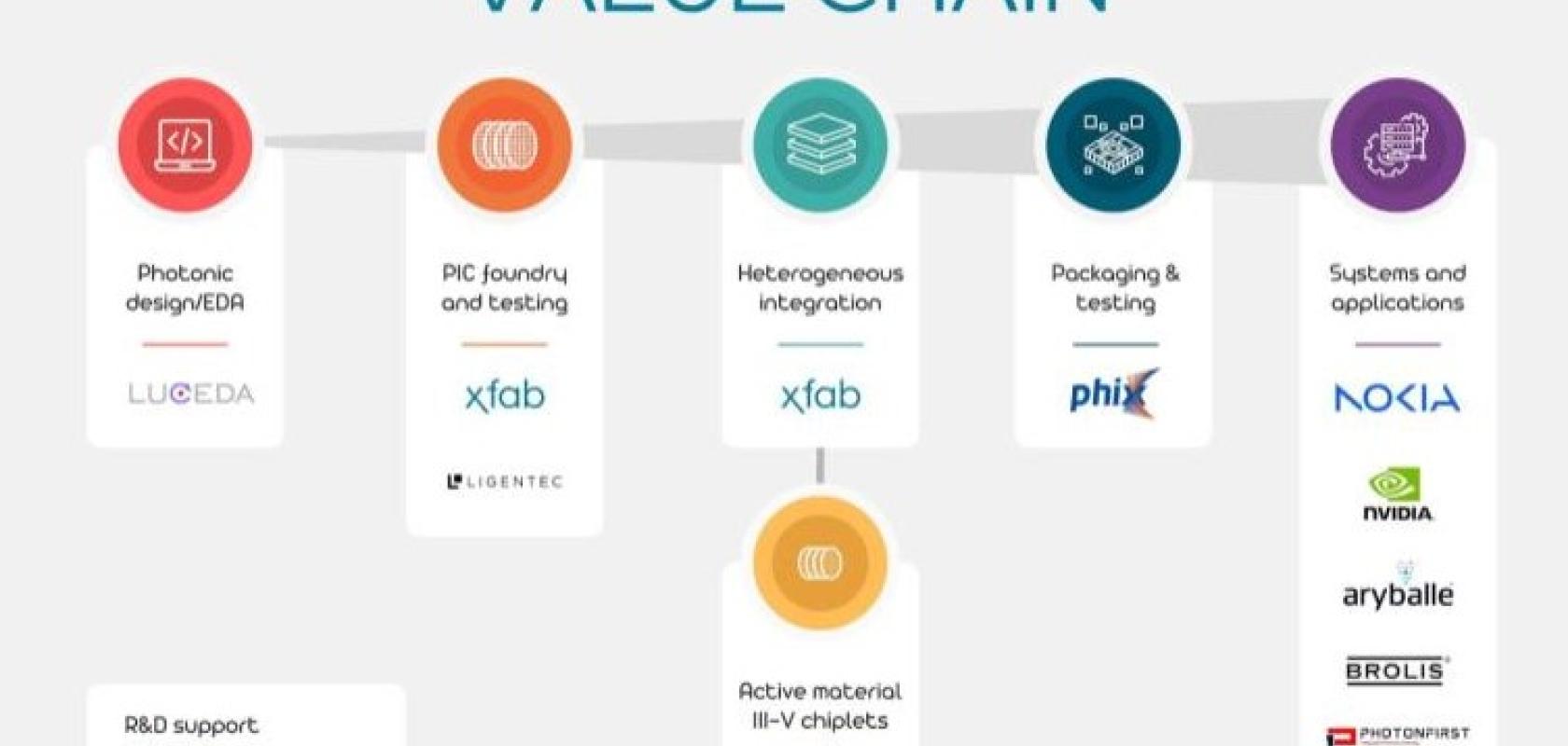
X-FAB, a leading analogue/mixed-signal and specialty foundry, will lead the European consortium, which covers the main part of the silicon photonics value chain, from design automation via foundry service all the way to end users.
Other consortium members include: technology and manufacturing service providers Ligentec, Smart Photonics, Phix Photonics Assembly and Luceda Photonics; application developers Nokia, NVidia, Aryballe, Brolis Sensor Technology and PhotonFirst; as well as major research organisations CEA-Leti and imec.
A multitude of prospective opportunities for the cutting-edge photonic devices fabricated via photonixFAB have already been identified. Among them are data communication, telecoms, biomedical sensors/detectors, quantum computing and vehicle lidar.
Rudi De Winter, CEO of X-FAB says: “Seeing huge potential emerging there, traditional semiconductor vendors, OEMs and start-ups are all now exploring photonic-enabled applications. Consequently, this is the right time for companies to work together on building an extensive Europe-centric silicon photonics ecosystem that will help drive the continent’s competitiveness in this exciting new market.”
Thomas Hessler, CEO of Ligentec, adds: “Europe has a leading edge in the research of PICs. photonixFAB is the next necessary step to turn this technology lead into a world leading industry, contributing to the strategic autonomy of Europe.”
Ligentec will focus on the advancement of its low loss SiN PIC platform, recently installed at X-FAB and now commercially accessible as 200mm wafer technology. A key outcome of the project will be an improved offering for agile prototyping with a seamless transfer to volume production. Ligentec will also work within the consortium on the integration of lasers, high speed modulators and detectors, by adding III-V material based active devices and electro-optical materials such as LNO to the low loss SiN PIC platform.
Meanwhile, Luceda Photonics will look to establish mature process design kits (PDKs) and commence bringing European PIC technologies to manufacturing. The integration of a highly automated design flow will play a pivotal role in this value chain.
Pieter Dumon, Luceda Photonics’ CTO: “Considering the substantial investment required for the development and manufacturing of photonic integrated circuits (PICs), a reliable and automated design flow is of essential importance. Through this project, we aim to set a major step toward PIC design based on well-calibrated simulation models, seamlessly integrated with Luceda’s automated design flow, thus minimising errors and ensuring efficiency.”
The project is being supported by the Key Digital Technologies Joint Undertaking (KDT JU), with funding from EU and the national authorities. The combination of this funding and the investments being made by each of the consortium members totals €47.6m.
