
One of the most interesting recent developments in this area is a research project carried out at Princeton University and NEC Labs America on the development of a silicon photonic-electronic neural network that could enhance submarine transmission systems.
As Chaoran Huang, visiting research scholar at Princeton University and assistant professor at the Chinese University of Hong Kong, explained, the novel system uses silicon photonic technologies, which provide ‘a most highly scalable platform for photonic integrated circuits because it offers high-quality photonic interconnects, while also delivering high-speed active components with competitive integration on the largest diameter wafers in production’.
Based on this technology, the project team developed a silicon photonic neural network chip to emulate the underlying neural network model with a so-called ‘broadcast-and-weight protocol’ demonstrated by the research group at the Princeton Lightwave Lab. This protocol uses the concept of wavelength division multiplexing (WDM) to enable scalable interconnections between photonic neurons. Neurons in this architecture produce optical signals with distinct wavelengths. These photonic neurons are multiplexed into a single waveguide and broadcast to all others.
‘Weights are applied to signals encoded on multiple wavelengths using groups of tunable wavelength filters. Tuning a filter along its transmission edge alters the transmission of each signal through that filter, effectively multiplying the signal with a desired weight. The resulting weighted signals are sent to a photodetector, which can receive multiple wavelengths in parallel and perform a summing operation on them,’ said Huang.
The generated photocurrent drives an optical modulator, which translates a nonlinear conversion of electrical photocurrent into optical power. As a result, optical modulators act as the nonlinear activation function – that is, the ‘neuron’ – in the photonic neural network.
‘These photonic devices have unmatched speed and bandwidth,’ said Huang. ‘As a result, algorithms running on the photonic neural networks (PNNs) could break performance limitations in electronics, and gain advantages in speed, latency and power consumption in solving intellectual tasks that are unreachable by conventional digital electronic platforms.
‘This is perhaps the first real-world application of photonic neural networks, and shows how the system can process optical signals in real time – that is, predicting and compensating for fibre nonlinearities in an over 10,000km trans-pacific submarine transmission link,’ she added.
Alternative hardware solutions
In view of the fact that today’s network traffic is ‘growing at a rate of 30 per cent annually’, Huang stressed that an increase in optical communications capacity of more than an order of magnitude ‘will be needed within the next decade to sustain the continued operation of the internet’. Moreover, signal distortions caused by detrimental effects in optical fibres ‘become more severe in high-capacity and long-distance communication systems’.
Huang explained ‘Digital signal processing (DSP), with its proven ability to combat transmission distortions, is a key technology that enabled the growth of the internet in past decades. However, the advances in high-speed DSP implemented CMOS electronic chips were heavily reliant on Moore’s Law scaling. Today’s semiconductor technology has approached the limits in terms of power dissipation, density and feasible engineering solutions. DSP capacity will therefore find it increasingly challenging to support the continued exponential growth of internet traffic in the post-Moore’s Law era,’ said Huang.
In recognition of this limitation, Huang pointed out the key objective of the research is to develop alternative hardware solutions that can address the potential optical network capacity crunch caused by the slowdown of Moore’s Law – prompting the team to use a neural network implemented in hardware on an integrated photonic chip enabled by silicon photonics, which emulates the underlying neural network model with photonic devices and circuits.
When compared with existing approaches, Huang observed that a key advantage of using the neural network for optical communications is that ‘a simple photonic chip with just a few neurons and tens of devices can, in principle, outperform commercial DSP chips in throughput, latency and energy use.
‘In addition, our photonic neural networks make use of high-quality waveguides and photonic devices – that is, photodetectors and modulators – that are originally designed for optical communications. As a result, the photonic neural networks can always accommodate fibre communication rates and enable real-time processing for future optical networks, promising to address the potential optical network capacity crunch caused by the slowdown of Moore’s Law,’ she said.
Seamless interface
Although the current work is focused on addressing the signal distortions in a single wavelength channel, Huang points out that the photonic neural network can also interface ‘seamlessly’ with WDM optical fibre systems. Moving forward, the research team plans to use this novel architecture to process multiple WDM channels in parallel and in the optical domain. According to Huang, this would result in a bandwidth increase ‘over Terahertz, significantly beyond the capability of DSP’.
‘This unique feature helps with inter-channel, nonlinear compensation in a WDM communication system, which DSP struggles with, while offering low-energy operation by eliminating power-hungry ADCs – which may consume more than 40 per cent of the energy in some transmission systems,’ she said.
‘Meanwhile, photonic neural networks, with their unique advantages in bandwidth, latency and power consumption, can play a unique role in enabling many new domains of applications – for example, machine learning acceleration, nonlinear programming [and] intelligent signal processing. Our future research will explore more applications of our photonic neural networks and we are working with NEC to figure out the commercialisation plans,’ she added.
Indium phosphide
Infinera has invested in building its own state-of-the-art InP PIC fabrication facility
Another interesting ongoing initiative is Infinera’s work on the development of high-performance indium phosphide (InP) as a platform for PICs for optical communications. Building on its reputation as an early pioneer in the field of photonic integration that built the industry’s first large-scale PIC in 2005, the company is now focused on leveraging high- InP-based PICs that integrate a wide range of optical functions on a single chip. As Paul Momtahan, director – solutions marketing at Infinera, explained, this approach ‘reduces cost, footprint and power consumption while improving performance and reliability.
‘We have also invested heavily in building our own state-of-the-art InP PIC fab – the only equipment manufacturer to have done so to date. In addition to the obvious cost advantages of this vertical integration, it enables fast redesigns for optimised performance, tight quality control and a faster ramp to volume for new technologies and products, such as ICE6,’ he said.
In Momtahan’s view there are a number of inherent advantages to using Indium Phosphide in PICs and optical communications systems. To begin with, in terms of the modulator, he points out that InP’s electro-optic effect is ‘fundamentally more efficient than the plasma dispersion effect used by silicon photonics’ – and produces a phase change ‘up to 10 times higher for a given unit length and voltage, resulting in more compact and power-efficient modulators with lower loss, better linearity, larger modulation voltage for higher transmitter signal to noise, and therefore better reach.’
‘For this reason, as far as I am aware, all fifth-generation 90+ GBd coherent optical engines currently on the market use an InP modulator,’ he said.
Momtahan also observed that InP can support gain elements, such as laser and amplification – semiconductor optical amplifiers – enabling what he describes as ‘more monolithically integrated photonic circuits with better performance and lower cost’. He highlighted the fact that, in ‘pluggables,’ this capability also enables higher transmit power (0 dBm compared to –10 dBm) in QSFP-DD form factors since ‘they do not have room for an external micro-EDFA, which is key for compatibility with the many existing DWDM line systems’.
He added: ‘By comparison, silicon photonics relies on external (InP) lasers and amplifiers.’
When it comes to challenges, Momtahan observes that it takes ‘time, expertise and up-front investment’ to establish an indium phosphide manufacturing facility capable of delivering commercial volumes of high-performance coherent InP-based PICs.
‘For vendors that do not have experience with indium phosphide-based PICs, and do not own or have access to an indium phosphide fab, the ability to leverage existing CMOS foundries with legacy (~130nm to 45nm process node) equipment provides an option for vendors to bring photonic integrated circuits to market more quickly and with a lower up-front investment,’ he added.
In terms of current and potential telecoms applications, Momtahan observed that both InP and silicon photonics will continue to be used in coherent DWDM embedded and pluggable optical engine designs – but stressed that, for high-end embedded optical engines, superior modulation effect and greater photonic integration give indium phosphide an ‘inherent performance advantage’.
He added: ‘For coherent pluggables, InP’s ability to integrate amplification into the photonic integrated circuit enables higher transmit power in a QSFP-DD form factor relative to silicon photonics.’
Moving forward, Momtahan confirmed Infinera is investing in InP PICs for its embedded optical engines – enabling evolution to ‘even higher baud rates’ – and continues to invest in InP PICs for coherent pluggables, including the ICE-XR line of XR optics coherent pluggables.
Polymer PIC systems
Elsewhere, Colorado-based technology platform company, Lightwave Logic is exploring the use of high-performance optical polymers as part of polymer PIC systems for telecoms applications. Building on its experience in organic materials, particularly those with electro-optical properties, the company has refined its proprietary chromophore materials for a range of applications, including fibre optic communication.
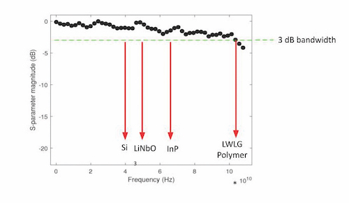
A relative comparison of modulator bandwidth (Lightwave Logic)
As Michael Lebby, CEO at Lightwave Logic, explained, some key properties of the materials include ‘low loss at 1310nm and 1550nm wavelengths, a high pockels effect, high glass transition temperature and excellent material stability.’ When the electro-optic polymers are fabricated into Mach Zehnder optical modulators – a device that is common in the internet – and optical networks, Lebby observed that ‘extremely fast optical switching speeds and low drive voltages are achieved’.
Although other semiconductor-based Mach Zehnder modulators are in commercial use today, Lebby said they suffer from ‘relatively low speed of operation and significantly higher power consumption through their higher voltage drive’ – restricting the industry on a plateau of modulator device speed and power consumption for the past decade.
‘We are now at a point in time where the PIC chips need to be turbo-boosted,’ he said. ‘The existing semiconductor modulators are simply not fast enough, and consume too much power. Our Polymer Plus optical polymer platform addresses these issues directly by allowing electro-optic polymers to be fabricated using standard silicon semiconductor techniques. For example, the polymer material can be spun onto silicon photonics circuits, so that the polymer modulators increase the speed of the PIC chip, while keeping power consumption low.’
He added: ‘Our Polymer Slot technology can also be fabricated into a PIC platform with increased performance and with a very small footprint, saving cost through the use of less real estate. It doesn’t matter if the transceiver is pluggable or on-board, both need high-speed modulation at lower power consumption levels.’
For Lebby, the performance advantages of using electro-optic polymers ‘can be seen through the performance Mach Zehnder modulator devices’ – with modulators featuring the material ‘easily achieving’ electro-optical bandwidths of 70-100GHz, two to three times more than existing semiconductor devices. Moreover, when the modulators are driven at one volt or less, Lebby observes that the low voltage ‘eliminates the need for dedicated drivers, which in turn allows the optical system architect to drive directly from the CMOS electronics, saving the system power and money’.
Although both the Polymer Plus and Polymer Slot technology platforms are currently based on the use of large CMOS silicon foundries – fabrication plants that focus on silicon semiconductors, and have traditionally set up their process design kits (PDKs) for integrated circuits (ICs) – Lebby revealed that, over the past few years, many silicon foundries have been ‘looking at increasing their wafer throughput by servicing silicon photonics solutions’.
He said: ‘It is these foundries that are the catalyst for volume scale when polymers are added to silicon photonics. Electro-optic polymers are being used to create polymer modulators at our facility in Colorado, and in a small fabrication plant. Transporting the standard semiconductor fabrication techniques to a large foundry in terms of a PDK is relatively straightforward, as the processes are amenable.’
To make polymer modulators ‘ubiquitous across the industry’, Lebby also pointed out that challenges are being addressed at ‘record pace’ – including advanced and mature electro-optic polymers, simple and standard fabrication in large-scale volumes, and packaged modulator device implementation into commercial applications.
‘The polymer industry for fibre communications is growing quickly, and with the correct positioning for scale, volume and performance, electro-optic polymers are poised very well to enable optical network system businesses to be much more competitive,’ he added.