A team of researchers from Duke University and Facebook’s Connectivity Lab have created a new plasmonic metasurface that achieves record high light efficiency over the entire centimetre-scale metasurface.
This advance means that the new nanostructured thin film can be used in applications from optical communications to fluorescence-based biosensing.
The research, which was published in Optica, The Optical Society's (OSA) research journal, detailed how the team designed nanostructured metasurfaces that boost the intensity and speed at which light is absorbed and emitted as fluorescence through surface plasmon resonance. Surface plasmon resonance occurs when certain wavelengths of light interact with free electrons at the interface of a metal and an insulator, or dielectric, surface.
Research team leader Maiken Mikkelsen from Duke University explained: ‘The major obstacles for using plasmonic structures for practical applications is that they are either too inefficient or their nanoscale properties aren't easily scalable to larger sizes. We designed and optimised a plasmonic metasurface that overcomes both of these limitations. Our work shows that plasmonic structures can be very useful for enhancing both absorption and emission of light, not just from tiny nanocavities but over large wafer-scale areas. This could be useful for ultrafast optoelectronics devices used in communications applications and could also increase the sensitivity of fluorescence-based biosensors.’
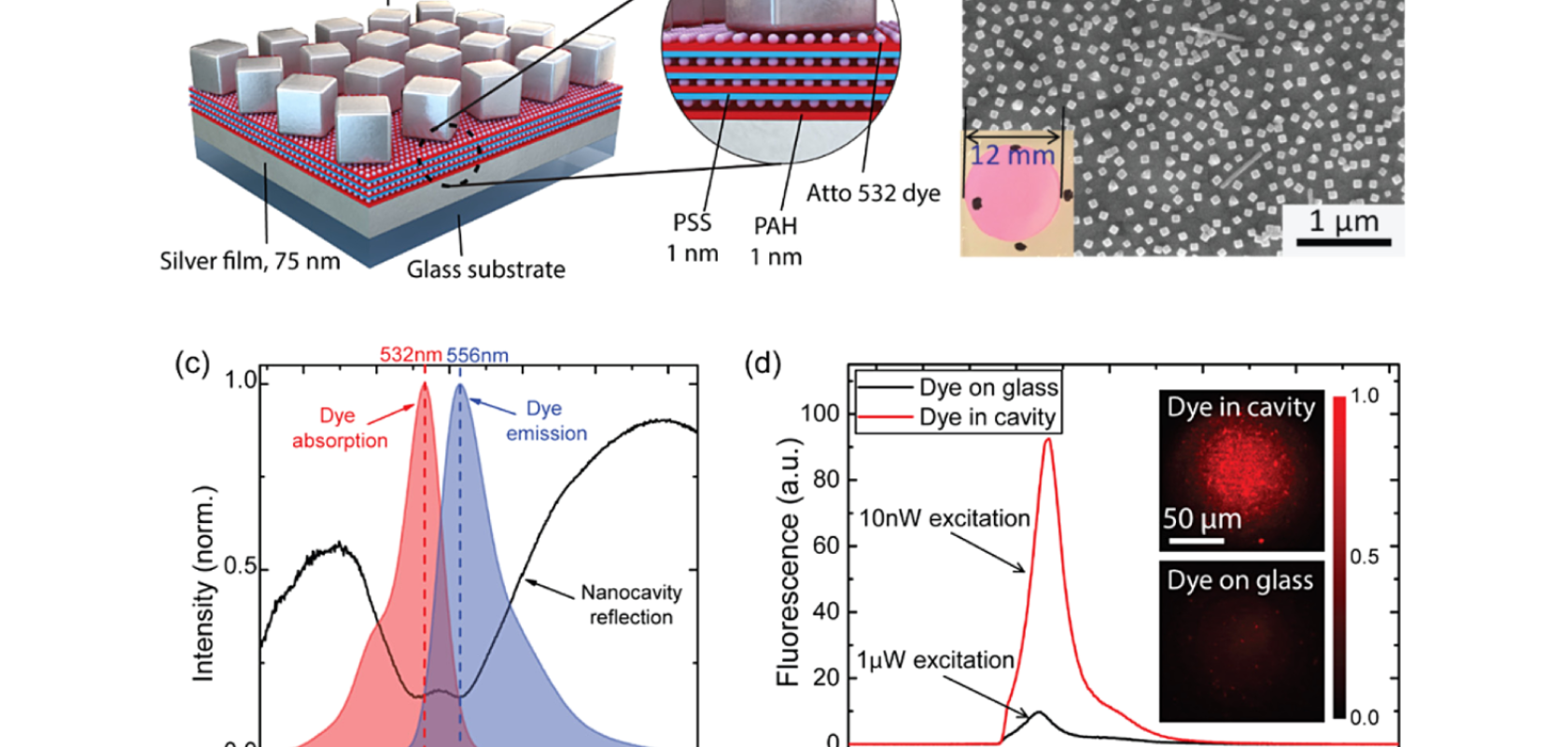
To create the film, the researchers developed a nanostructure that sandwiched fluorescent dye molecules between a gold film and 100nm wide silver cubes. When light hits the structure, it excites localised surface plasmons, enhancing the electromagnetic field around the dyes, causing them to emit light very quickly after being excited by the incoming light.
By putting just 10nm between the film and the nanocubes, the researchers found that they could dramatically increase the spontaneous emission rate of the entire metasurface wafer. To increase efficiency even more, they used multiple layers of dye.
Tests of the new metasurface showed that it exhibited record high overall efficiency of about 30 per cent for converting the incoming excitation light into emitted fluorescence. The nanoscale structures also maintained a light modulation rate of more than 14GHz across the full centimetre-scale metasurface, which the team says has never been demonstrated before. This is particularly interesting for optical communications applications, where faster light modulation allows more data to be encoded into light signals at a higher rate.
