University of Utah engineers have developed an ultra-compact beamsplitter – the smallest on record – for dividing light waves into two separate polarisations along separate paths.
The device brings researchers closer to producing complex silicon photonic chips that compute and shuttle data with light instead of electrons.
“Light is the fastest thing you can use to transmit information,” said Menon. “But that information has to be converted to electrons when it comes into your laptop. In that conversion, you’re slowing things down. The vision is to do everything in light. With all light, computing can eventually be millions of times faster.”
The compact beamsplitter could be particularly useful in photonic devices that are strongly birefringent, where their optical performance is polarisation dependent, such as those made in silicon-on-insulator material systems. A polarisation beamsplitter would allow the two polarisation states to be processed independently.
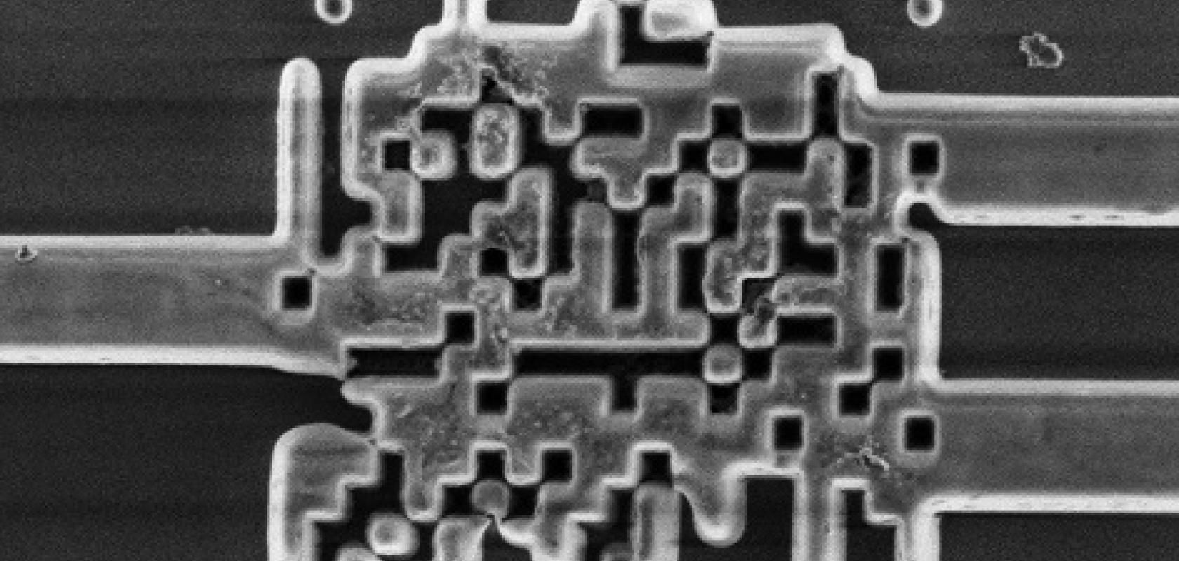
To help do that, the Utah engineers created a much smaller form of a polarisation beamsplitter (which looks somewhat like a QR-code) on top of a silicon chip that can split guided incoming light into its two component polarisations.
Before, such a beamsplitter measured more than 100 by 100 microns. Thanks to a new algorithm for designing the splitter, Menon’s team has shrunk it to 2.4 by 2.4 microns, almost 50 times smaller, and close to the limit of what is physically possible.
The Utah researchers then characterised their device and showed experimental TE and TM transmission efficiencies of 71 and 80 per cent, respectively.
The beamsplitter would be just one of a multitude of passive devices placed on a silicon chip to direct light waves in different ways. By shrinking them down in size, researchers will be able to cram millions of these devices on a single chip.
Potential advantages go beyond processing speed. The Utah team’s design should be cheap to produce because it uses existing fabrication techniques for creating silicon chips. The waveguides and patterned area could be processed in the same step.
A likely first application is supercomputers using silicon photonics — already under development at companies such as Intel and IBM — using hybrid microprocessors that remain partly electronic. Menon believes his beamsplitter could be used in those computers in about three years. Data centres that require faster connections between computers also could implement the technology soon, he says.
The work was published in the journal Nature Photonics.