PIC your test to deliver reliable optical component performance in a next-generation world, says François Couny
The extensive use of photonics integrated circuits (PICs) driven by advanced networking technologies has significant implications for testing the key components that underpin today’s telecom networks.
The 2020 telecom world sees proliferation of 5G globally, an increase in network and data centre rates to 400G, greater bandwidth and energy efficiency requirements for high-speed networks, and ongoing and escalating demand for compact, connected devices. Component vendors need faster and more reliable test methods than ever before to keep pace with this burgeoning demand and to accommodate new optical component characteristics.
With the goal of addressing pain points for telecom vendors, PIC technology has arguably revolutionised the components industry by enabling a mix of optical and electronic functionalities on a single chip, reducing size, power consumption, and cost while boosting reproducibility and yield. But the sheer volume of PIC components that require testing, plus the need for accurate testing at every stage of design, fabrication, assembly, and packaging creates daunting challenges for manufacturers.
To ensure peak performance, solutions have been developed to ensure the speed and reliability of PIC testing both in the manufacturing process and in deployment.
Today’s networks
The telecom industry has been using PIC technology for more than a decade in such devices as semi-conductor optical amplifiers, Mach-Zehnder (MZ) modulators, coherent transceivers, and tunable lasers. The efficiency, scalability, high manufacturability, and constantly decreasing form factor of PIC components will continue to make them crucial as next-generation networks are deployed.
The increased density on cell sites and base stations, more fibre installed than ever before, and more components and PICs to help process the increase in data, makes optimum PIC performance crucial. Testing is an integral part of each stage in a PIC project, so much so that TAP (test, assembly and packaging) constitutes up to 80 per cent of the total cost of PIC production.
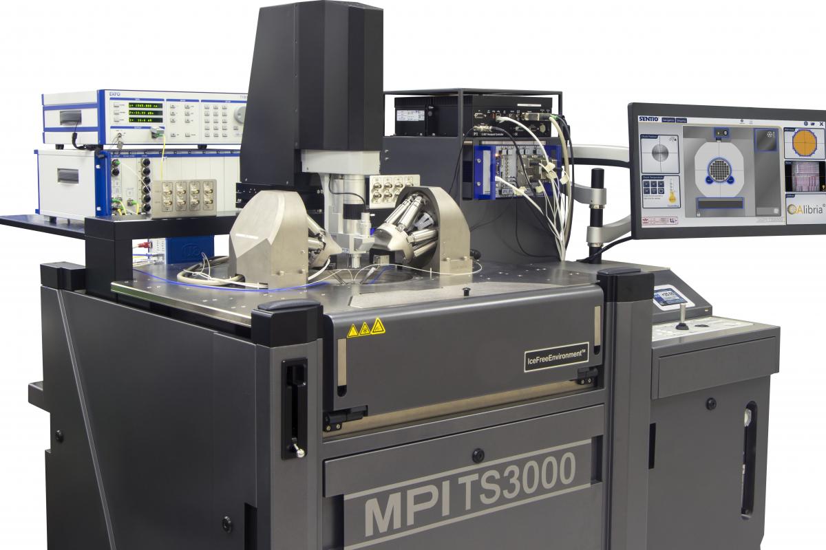
The fundamental characteristic of an optical component is its spectrum, and parametric testing is performed at an early stage to avoid integrating defective devices. As a result, parametric tests should be performed on PICs at the wafer level, prior to wafer cutting and packaging, so that hundreds of PICs can be characterised and automatically selected, and faulty components eliminated.
Traditional methodologies
The goal for manufacturers is to ensure that all PICs are tested using a consistent, uncomplicated method that produces accurate and reliable results. This sounds straightforward, but testing key parameters on the multitude of active and passive optical, electronic, or RF components contained on each chip can be demanding. Here are the methods currently used for active and passive component testing.
For active component testing
An optical spectrum analyser (OSA) provides fast spectral measurement of light sources such as lasers. Leading OSAs are capable of performing up to five scans per second at speeds of 2000nm/sec., fast enough for real-time component alignment and with sufficiently high resolution to enable measurement of key parameters. This provides a simple and effective test method for active component testing.
For passive component testing
An OSA can be used with a broadband light source with very large, flat spectrum, and stable power. When combined with the chip, the light can be collected and coupled to the OSA which will then perform a sweep to record the spectral response of the device under test (DUT). This method is good for real-time alignment because it’s extremely fast; however, there are limitations to its scope. It works well for broadband components (with slowly varying spectrum) but fails in high-contrast spectrum scenarios. Given that PIC is often high contrast, the OSA method does not always provide the optimum solution.
Stepped laser technique can be used with a detection system comprising several hundred power meters. The dynamic range obtained with this technique is very wide due to the laser’s optical power density. This method provides good spectral coverage by using one or several lasers between 1250-1700 nm and easy-to-control polarization for performing polarization dependent loss (PDL) measurements.
The biggest limitation of the stepped laser technique is the lengthy time required, given that the laser must ‘stop’ at each wavelength to perform measurement.
Swept Laser testing for advanced reliability
The only test approach that is proving to lead the pack when it comes to delivering fast and reliable measurements for today’s complex components is the swept laser technique.
This elegant solution uses a continuously tunable laser source along with a component tester that records wavelength and power detection synchronously as the wavelength is scanned by the laser. Within seconds it can deliver picometer spectral resolution with a very large optical power dynamic range.
Quality component testers combine multiple lasers to cover the full range of optical components. The larger spectral range, important when characterizing components spanning all telecom bands, can indeed be tested using several tunable lasers – each of which covers a portion of the total spectrum under test – and concatenating the insertion loss or return loss result into a single spectrum.
To match the high quality of the laser, the component tester must be leading-edge, providing very short test times and excellent accuracy to record the test wavelength and output power simultaneously as the laser is being swept. This synchronised measurement is performed automatically by the component tester. The component tester can also be automated to allow, for example, ‘fixed wavelength’ power measurement which is crucial for the fast fibre-to-PIC alignment algorithm.
Future-ready testing
Tiny but powerful PICs are fuelling the future of telecom, unlocking the best of photonic and electronic worlds by merging purely optical components such as lasers and modulators with opto-electronic, electro-optical, fully electronic, or even RF features. The result is a chip with endless potential in applications ranging from data centres to medicine, and from autonomous cars to quantum computing.
The key to success will be innovative, reliable, and speedy optical component test solutions to keep pace with next-generation networking technology. With ultra-fast optical spectrum analysers and optimized swept laser technique, component manufacturers are well positioned to deliver during the ongoing bandwidth boom.
The extensive use of photonics integrated circuits (PICs) driven by advanced networking technologies has significant implications for testing the key components that underpin today’s telecom networks.
The 2020 telecom world sees proliferation of 5G globally, an increase in network and data centre rates to 400G, greater bandwidth and energy efficiency requirements for high-speed networks, and ongoing and escalating demand for compact, connected devices. Component vendors need faster and more reliable test methods than ever before to keep pace with this burgeoning demand and to accommodate new optical component characteristics.
With the goal of addressing pain points for telecom vendors, PIC technology has arguably revolutionised the components industry by enabling a mix of optical and electronic functionalities on a single chip, reducing size, power consumption, and cost while boosting reproducibility and yield. But the sheer volume of PIC components that require testing, plus the need for accurate testing at every stage of design, fabrication, assembly, and packaging creates daunting challenges for manufacturers.
To ensure peak performance, solutions have been developed to ensure the speed and reliability of PIC testing both in the manufacturing process and in deployment.
Today’s networks
The telecom industry has been using PIC technology for more than a decade in such devices as semi-conductor optical amplifiers, Mach-Zehnder (MZ) modulators, coherent transceivers, and tunable lasers. The efficiency, scalability, high manufacturability, and constantly decreasing form factor of PIC components will continue to make them crucial as next-generation networks are deployed.
The increased density on cell sites and base stations, more fibre installed than ever before, and more components and PICs to help process the increase in data, makes optimum PIC performance crucial. Testing is an integral part of each stage in a PIC project, so much so that TAP (test, assembly and packaging) constitutes up to 80 per cent of the total cost of PIC production.
The fundamental characteristic of an optical component is its spectrum, and parametric testing is performed at an early stage to avoid integrating defective devices. As a result, parametric tests should be performed on PICs at the wafer level, prior to wafer cutting and packaging, so that hundreds of PICs can be characterised and automatically selected, and faulty components eliminated.
Traditional methodologies
The goal for manufacturers is to ensure that all PICs are tested using a consistent, uncomplicated method that produces accurate and reliable results. This sounds straightforward, but testing key parameters on the multitude of active and passive optical, electronic, or RF components contained on each chip can be demanding. Here are the methods currently used for active and passive component testing.
For active component testing
An optical spectrum analyser (OSA) provides fast spectral measurement of light sources such as lasers. Leading OSAs are capable of performing up to five scans per second at speeds of 2000nm/sec., fast enough for real-time component alignment and with sufficiently high resolution to enable measurement of key parameters. This provides a simple and effective test method for active component testing.
For passive component testing
An OSA can be used with a broadband light source with very large, flat spectrum, and stable power. When combined with the chip, the light can be collected and coupled to the OSA which will then perform a sweep to record the spectral response of the device under test (DUT). This method is good for real-time alignment because it’s extremely fast; however, there are limitations to its scope. It works well for broadband components (with slowly varying spectrum) but fails in high-contrast spectrum scenarios. Given that PIC is often high contrast, the OSA method does not always provide the optimum solution.
Stepped laser technique can be used with a detection system comprising several hundred power meters. The dynamic range obtained with this technique is very wide due to the laser’s optical power density. This method provides good spectral coverage by using one or several lasers between 1250-1700 nm and easy-to-control polarization for performing polarization dependent loss (PDL) measurements.
The biggest limitation of the stepped laser technique is the lengthy time required, given that the laser must ‘stop’ at each wavelength to perform measurement.
Swept Laser testing for advanced reliability
The only test approach that is proving to lead the pack when it comes to delivering fast and reliable measurements for today’s complex components is the swept laser technique.
This elegant solution uses a continuously tunable laser source along with a component tester that records wavelength and power detection synchronously as the wavelength is scanned by the laser. Within seconds it can deliver picometer spectral resolution with a very large optical power dynamic range.
Quality component testers combine multiple lasers to cover the full range of optical components. The larger spectral range, important when characterizing components spanning all telecom bands, can indeed be tested using several tunable lasers – each of which covers a portion of the total spectrum under test – and concatenating the insertion loss or return loss result into a single spectrum.
To match the high quality of the laser, the component tester must be leading-edge, providing very short test times and excellent accuracy to record the test wavelength and output power simultaneously as the laser is being swept. This synchronised measurement is performed automatically by the component tester. The component tester can also be automated to allow, for example, ‘fixed wavelength’ power measurement which is crucial for the fast fibre-to-PIC alignment algorithm.
Future-ready testing
Tiny but powerful PICs are fuelling the future of telecom, unlocking the best of photonic and electronic worlds by merging purely optical components such as lasers and modulators with opto-electronic, electro-optical, fully electronic, or even RF features. The result is a chip with endless potential in applications ranging from data centres to medicine, and from autonomous cars to quantum computing.
The key to success will be innovative, reliable, and speedy optical component test solutions to keep pace with next-generation networking technology. With ultra-fast optical spectrum analysers and optimized swept laser technique, component manufacturers are well positioned to deliver during the ongoing bandwidth boom.
François Couny is product line manager at EXFO