Photon Bridge has announced wafer-scale validation of its heterogeneous photonics platform for multi-wavelength light engines, demonstrating single-channel output power exceeding 30mW at silicon chip edge facets in continuous-wave operation at room temperature.
The Netherlands-based company said the demonstrated power levels meet per-channel requirements for next-generation 1.6 Tbit/s and 3.2 Tbit/s co-packaged optical (CPO) engines. This enables reduced fibre count and improved rack-level energy efficiency in AI-driven data centre deployments.
Multi-wavelength architecture reduces fibre count
While traditional non-multiplexed external laser source (ELS) solutions deliver one colour per fibre using high-power 250mW lasers, Photon Bridge's platform achieves comparable aggregate per-fibre output by combining multiple wavelengths on a single fibre. By integrating lasers and multiplexing functions on a single silicon photonics interposer, the platform reduces fibre count, simplifies assembly and improves thermal efficiency.
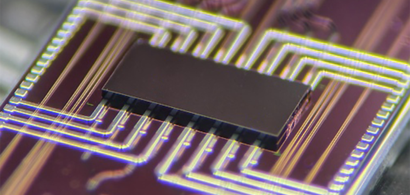
The milestone validates a fully integrated architecture in which lasers and wavelength filters reside on a single silicon photonic integrated circuit (PIC), eliminating discrete micro-optics and simplifying assembly. The platform leverages established commercial III-V and 200 mm silicon photonics foundries, enabling what the company describes as scalable and cost-effective deployment.
Manufacturing optimised for volume production
Unlike conventional III-V-on-silicon approaches that depend on tight manufacturing tolerances and complex test flows, Photon Bridge's platform is designed for volume production. A simplified silicon photonics process and outsourced semiconductor assembly and test (OSAT)-compatible assembly reduce III-V laser integration time by up to 80 times, according to the company.
Initial wafer-scale testing demonstrated robust III-V to silicon interface connectivity, with more than 92% of interconnections meeting performance specifications.
Paul Marchal, CEO of Photon Bridge, said the results validated both power handling and manufacturability: "The architecture scales to 8, 16 or 32 wavelengths per fibre and can extend across multiple fibres to achieve significantly higher aggregate output power, without driving individual lasers to extreme power densities. With scalability demonstrated, we are now focused on industrialisation and customer qualification for high-volume deployment."
Quantum dot roadmap
The platform is designed to scale to quantum dot laser technology, offering the potential for isolator-free operation and further simplifying system-level design for high-density optical engines.
Photon Bridge's patented cantilever waveguide platform unifies lasers, silicon photonics and optical control into a single production-ready architecture, designed for compatibility with commercial foundries and OSAT assembly flows.
OFC 2026
The Photon Bridge team will be at OFC Conference in Los Angeles from 17 to 19 March 2026, at booth 757.
Are you interested in optical interconnect for AI-driven data centre deployments? Register for our free upcoming webinar!