Before silicon photonics can fulfil its commercial potential – providing low-cost, high-speed optical devices for connecting servers and switches inside data centres – it must overcome many challenges. One is getting the chips made. The technology is well established, but the manufacturing processes have yet to reach a level of maturity sufficient to enable silicon photonics to make a seamless transition to industrial-scale production.
That’s a big deal, considering that the real promise of silicon photonics lies in the potential to exploit the low-cost, high-volume manufacturing processes of the microelectronics industry. It also represents an unfortunate barrier to start-ups and smaller businesses wanting to enter the market.
Multi-project wafer (MPW) programs have long been considered an economical way to produce low-volume photonic integrated circuit (PIC) prototypes by integrating designs from different teams onto a single wafer, but this is not enough. ‘Although an excellent vehicle for early-stage device fabrication, multi-project wafer runs offer limited volume capabilities,’ notes Peter O’Brien from Tyndall National Institute in Cork, Ireland. In addition, as they operate on a cost-share model, it can take several months to have devices fabricated.
Packaging of the devices is also a significant hurdle, typically accounting for more than 50 per cent of the final product cost, he adds. ‘It can be a major bottleneck in the production process, especially due to the technical challenges of precision alignment of optical fibres,’ O’Brien noted. Silicon photonics also has unique optoelectronic testing requirements that need to be addressed and optimised.
Companies have now ‘naturally progressed’ to PICs, O’Brien says. He cites an example of one firm that ‘knew nothing about integrated photonics’, but realised it would be more cost effective and robust to mechanical vibrations. ‘We were able to work with them and package prototypes,’ O’Brien recalled. ‘The big issue then comes when you show early prototypes to your customers. They’re immediately looking for scale-up: What do you do next?’
European efforts
To resolve the operational and business challenges involved in creating an ecosystem for silicon photonics manufacturing, research organisations like the Tyndall National Institute are working with companies like Geneva, Switzerland-headquartered STMicroelectronics, largely through European Union (EU) research programmes.
Among the first steps was the ePIXfab platform, which was ‘probably the world’s first’ MPW broker service in silicon photonics in 2006, according to Roel Baets from Ghent University in Belgium. ePIXfab mediated between designers and the fabs that produced their chips, which include imec, the Leuven, Belgium, electronics research institute (where ePIXfab chairperson Baets also works), and Leti in Grenoble, France.
The EU Europractice service took over the broker role in 2015, supporting both research and small volume production, Baets says, and the problem of long turn-around times is slowly improving. ePIXfab now operates as the European alliance for silicon photonics, with a mission to advance the field on behalf of more than 30 members.
But broker services don’t yet provide access to manufacturing-oriented industrial foundries. And going direct to fabs to process custom lots can be 5 to 10 times more expensive than participating in MPW platforms, even though the cost per chip reduces, according to Baets.
However, the situation has improved dramatically in recent years. There is now a European manufacturing ecosystem suitable for silicon PICs, says Christophe Kopp, head of Leti’s CMOS photonics laboratory. That’s thanks mainly to the EU’s PLAT4M (Photonic Libraries And Technology for Manufacturing) project, launched in 2012. It has helped develop the mature process that imec now offers on 200mm-diameter silicon wafers, together with a library of structures needed to produce 50Gb/s optical communication devices. Leti has established a more flexible 200mm process that includes heterogeneous integration of indium phosphide lasers onto silicon-on-insulator (SOI) wafers.
Meanwhile, STMicroelectronics has a mature 300mm process that uses multiple layers of silicon and silicon nitride, and also shares the same SOI platform as Leti. That means devices developed at Leti on 200mm wafers can be directly transferred to STMicroelectronics’ fab to be made on the larger 300mm wafers, Kopp says. During PLAT4M, both teams produced a 4×25G WDM datacom transceiver demonstrator using these platforms, and the development work continues under the French public-private partnership R&D initiative IRT NANOELEC.
Better by design
To successfully develop complex photonic circuits, high-performance component design is a primary requirement, emphasises Ségolène Olivier, R&D project leader in silicon photonics at Leti. That means going beyond the design of individual photonic components. Behavioural simulations of both photonic and electronic components must be developed to create ‘a mature design kit for complex PICs’. ‘Packaging aspects are also very important to include, in order to meet the standards of compact and low energy-consumption modules,’ Olivier observed.
Consequently, imec and Leti have devised process design kits alongside the silicon photonic processes that they developed in PLAT4M. These kits are available through electronic design automation platforms like US-headquartered Mentor Graphics’ Pyxis, and Dutch PLAT4M partner PhoeniX Software’s OptoDesigner. They’re also included in software from San Jose, California’s Cadence and Belgium-based Luceda. In addition, Mentor Graphics and imec have implemented Layout Versus Schematic (LVS) verification to reduce design errors, and design analysis to improve the predictability of lithographic patterning in silicon photonics.
Leti’s new silicon photonics process is now available via the Grenoble-based MPW broker CMP (Circuits Multi-Projets) and is attracting great interest from industrial R&D teams as well as academics. Yet that’s just a start. ‘What is needed today is for industrial foundries to offer MPW runs,’ said Kopp. STMicroelectronics, which offers MPW runs for microelectronics via CMP, is the obvious candidate. Kopp expects STMicroelectronics to make the common SOI platform it shares with Leti available, but he doesn’t yet know when. He adds that the supply chain also needs to offer lasers integrated into silicon PICs. ‘At Leti, we plan to propose it in MPW R&D runs within two to three years,’ Kopp said.
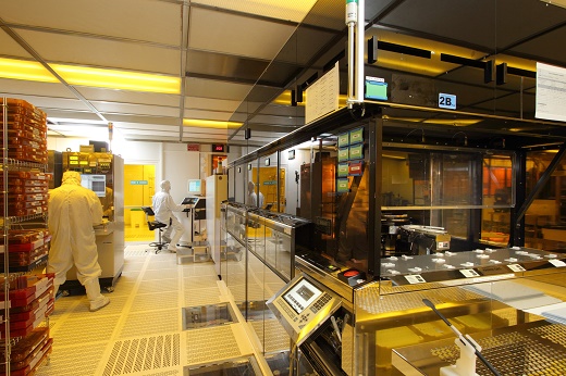
Looking into Leti's 200mm clean room in Grenoble, France
Foundry services are not the main priority for Frédéric Bœuf, silicon photonics technologies manager at STMicroelectronics’ fab in Grenoble, however. Instead he focuses on the company’s desire to ‘provide customers with best-in-class silicon photonics optical engines ready for packaging in optical modules’. ‘Currently we are shipping 100G-PSM4 compliant optical engines relying on our PIC25G silicon photonics technology and our B55 high-speed BiCMOS technology,’ he said. ‘Our next target, currently under development, is to address 200G and 400G application ranges.’
PLAT4M’s design efforts are helping resolve a key difference between silicon photonics and microelectronics processes that has made this harder, Bœuf emphasises. Microelectronics devices can usually be designed as ‘Manhattan’ structures, in a neat grid with 90˚ angles between all lines. By contrast, optical devices are typically more curved, which causes trouble in conventional computer-aided design tools when handling layout verification or optical proximity corrections.
‘In this area, strong progress has been made in recent years, in particular within the PLAT4M project,’ Bœuf said. ‘We also developed some new process modules, allowing more flexibility in optical component design than our current industrial technology.’ His firm is evaluating the simulation and design tools developed by PLAT4M for use in its next technology generations.
Demonstrating applications
With PLAT4M now complete, Bœuf says that STMicroelectronics ‘is interested in application-oriented European projects to explore new potential applications or technology breakthroughs with academic or industrial partners’. As an example, heterogeneous material integration on silicon is a promising way to extend device performance and application fields for silicon photonics, he adds. A project to develop pilot lines in Europe may be of interest for small and medium-sized enterprises (SMEs) willing to develop new concepts using an industrial fab.
One application-oriented European project is COSMICC, (CmOs Solutions for Mid-board Integrated transceivers with breakthrough Connectivity at ultra-low Cost), which started in December 2015, and is coordinated by Olivier. COSMICC aims to develop silicon photonics technology for 2km links inside data centres at aggregated data rates beyond 1Tb/s. STMicroelectronics’ 300mm process will be key in achieving this. Leti will also develop a more advanced generation of photonics components on its 200mm R&D platform, for later transfer to STMicroelectronics. It is working on advanced components and technology to integrate new materials and processes – the use of III-V compound semiconductor materials and silicon nitride will make it possible to integrate lasers and reduce sensitivity to temperature variations.
COSMICC’s academic partners include the University of Southampton and University of St Andrews in the UK, University of Paris Sud, France, and Cork Institute of Technology, Ireland. They’re developing advanced ultra-compact and ultra-low energy consumption silicon photonics modulators and photodetectors, aiming at prototype demonstrations, working closely with Leti and STMicroelectronics. The University of Pavia and STMicroelectronics are also developing high-speed, low-power electronic circuits to drive the PICs.
Another of COSMICC’s industrial partners – Seagate Systems in Havant, UK – will test transceivers in data centre scenarios. The partners representing the other links in the supply chain include Vario-optics, a Swiss start-up developing polymer ribbon waveguides that can be used to attach multiple optical fibres to the PIC at the transceiver inputs and outputs. The Berlin-based subsidiary of optical component manufacturer Finisar is also bringing its expertise in packaging and development of photonic modules, Olivier says.
‘Between the silicon photonics foundry players and end users deploying photonic solutions in data centres, industrial module vendors such as Finisar play a key role,’ Olivier stresses. ‘They will integrate silicon PICs into modules directly usable by data centre equipment manufacturers. It is therefore important to develop the entire value chain, from technology to silicon photonic products in data centres.’
COSMICC’s specific objective is to develop two mid-board transceiver module demonstrators for data centre switches. ‘The first demonstrator is a coarse WDM (CWDM) mid-board transceiver for 100Gb/s communications based on two channels at 50Gb/s and two fibres, one each for the transmitter and receiver,’ Olivier said. ‘That demonstration can be scaled to 400Gb/s with four pairs of fibres. Demonstrator development is in progress with PICs and electronic circuits already developed – results are expected by the end of the year.’
The second demonstrator is a CWDM mid-board transceiver with an aggregate data rate of 2.4Tb/s based on four CWDM channels at 50Gb/s on each of 24 fibres, 12 for the transmitter and 12 for the receiver. ‘Results concern mainly development of new advanced photonic components, like the design of low-consumption capacitive optical modulators and temperature-insensitive four-channel CWDM multiplexers/demultiplexers,’ Olivier said. ‘These components are the result of both design and technology innovations. They are key for the new generation of CWDM transceivers at the heart of our second demonstrator.’
Piloting progress
Firms other than STMicroelectronics wanting to bring such innovations to market must rely on foundries – and, even then, still have plenty to do to produce a finished product.
Since O’Brien joined the Tyndall National Institute in 2009, he has been pushing for better optoelectronic testing and packaging know-how. Having worked on several difficult-to-package devices that companies brought to them, his group developed a comprehensive set of packaging design rules.
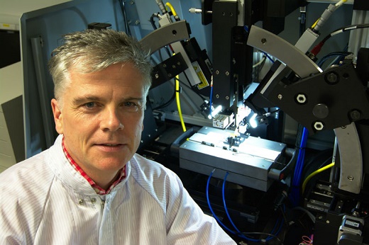
Peter O'Brien from Tyndall National Institute leads the PIXAPP project
O’Brien is now leading an EU pilot line project called PIXAPP, seeking to establish a low-medium volume PIC packaging pilot line targeting SMEs. It includes industrial partners able to scale-up to volume production. The PIXAPP pilot line is distributed among different institutions, with Tyndall serving as the gateway, and plans to be self-sufficient once its four years of funding are up, O’Brien stresses. He adds that in 2018, the EU will call for proposals for similar silicon and indium phosphide chip production pilot lines.
Crucially for such collaboration, the design rules Tyndall has devised have been made available by Europractice, and incorporated into some of the software environments created in PLAT4M. The pilot lines in PIXAPP are also producing silicon, indium phosphide and silicon nitride reference PICs that embody the same rules. ‘It’s like a Swiss Army knife of a chip, we’ve got everything that needs to be packaged,’ O’Brien said. The reference PICs can then be used to educate and assess packaging companies wanting to join the pilot line.
Through PIXAPP, Tyndall is training companies about photonic packaging equipment, prior to them buying such equipment for their own manufacturing facilities. In January the project will also offer what O’Brien calls a ‘unique’ week-long, in-lab training course when companies can bring in their work. ‘People can come in to do hands-on training on packaging, taking real PICs and learning,’ he explained.
Such efforts are attracting attention, with the US photonics manufacturing consortium AIM Photonics visiting Tyndall in mid-2017. ‘We’re happy to collaborate with AIM and other organisations, so we work from a common platform,’ O’Brien said. He believes progress in Europe has been largely driven by co-ordination – and he now hopes that mindset will spread globally. ‘That’s why we’re linking up with groups in the US, Japan and China,’ O’Brien said. ‘It’s very important that we work together towards a common objective.’
• Andy Extance is a freelance science writer based in Exeter, UK