Daniel Schall’s experiments in 2009 quickly demonstrated to him and his colleagues ‘that the optical properties of graphene were absolutely unique’. Together with results from Heinrich Kurz’s team at RWTH Aachen, Germany, Schall’s PhD findings at the nearby company that Kurz founded, AMO, promised great things.
‘The question was: can we build an electro-optic device like a photodetector or modulator?’ Schall recalls. By 2011, the team had waveguide-integrated devices ready, some based on large-scale CVD graphene, some based on graphene flaked from graphite. When, in 2014, AMO published several results on detectors and modulators ‘it became clear that the process steps involved should be possible on wafers’, Schall said. He and his colleagues demonstrated the first wafer-based results in 2015. ‘Today we have a graphene photonics platform and we fabricate more than a thousand devices on a wafer,’ Schall continued, including prototype photodetectors and modulators.
AMO is not doing this in isolation. It’s part of the Graphene Flagship project in Europe that started in 2013. The project aims to establish a supply chain intending to exploit the wonder material’s well-known properties, such as electron mobility over a hundred times greater than silicon. There remain practical and commercialisation hurdles to overcome, but progress so far has been promising.
‘Bandwidth is absolutely important in optical communication and graphene devices are naturally fast,’ explained Schall. ‘Graphene has this unique set of properties that do not require any alteration or manipulation for high performance electro-optic devices. Our next step is to come from research-level devices demonstrating certain performance, to real products. We expect graphene photodetectors to be marketable in the near future.’
Performance indicators
Nokia is also involved in the Graphene Flagship project. Wolfgang Templ, manager of the wireless transceiver research department at Nokia Bell Labs in Stuttgart, said that the company is interested in ‘future communication systems beyond 5G which need to deal with bitrates over 1Tb/s per optical channel.’ With its project partners, Nokia has started investigating graphene electro-optical and opto-electrical converters. ‘We integrate the components provided by our research partners into our communication systems and analyse and assess their performance,’ Templ said.
Such applications benefit from graphene’s high charge carrier mobility. ‘Graphene might get into an enabling role with a unique selling point if we succeed in maintaining its inherent properties during the device integration process,’ he said. ‘Moreover, based on the material’s electronic properties, graphene-based photonic components feature a wide spectral tuning range. This feature perfectly serves the needs of future dynamically reconfigurable networks.’
Yet Templ believes that delivering on theoretical predictions about the superior performance of graphene is the biggest challenge faced by the Graphene Flagship. ‘The properties of the pristine material predicted by theory degrade substantially when it comes to physical component realisation,’ he said. ‘The crystallographic quality of graphene layers is still not sufficient for achieving the required high carrier mobilities, and the contacts still feature too-high sheet resistance.’ As such, today’s graphene-based optical modulators are still behind the overall performance of equivalent InP or LiNbO3 devices, although Templ acknowledges that there is fast progress.
From lab to fab
Another important challenge is getting graphene component production from research labs into large-scale production. ‘Setting up mass production of components with reproducible high quality and good yield observing all the commercial requirements and constraints is a huge task on its own,’ Templ said. ‘The pilot line, initiated by the European Graphene Flagship project, is an important first step in that direction. But it will be necessary that large component manufacturers adopt the results and take over as soon as a certain level of maturity has been reached.’

Graphenea, in San Sebastián, Spain, is another Graphene Flagship member, supplying the graphene material in many cases, explains Amaia Zurutuza, the company’s scientific director. She highlights that using graphene in modulators and detectors for optical communications could reduce costs, as well as improving speed. Zurutuza recognises that graphene is more expensive than silicon, reflecting its small market. ‘As any material, it goes with economies of scale,’ Zuruzuta said. ‘In the history of Graphenea, since 2010 our prices have gone down dramatically. We don’t think this is going to be a limiting factor.’
Importantly, Graphenea’s processes are carefully engineered to fit with the existing semiconductor industry. ‘In order for graphene to be applied in most electronic or optoelectronic applications, you need to first grow it inside a CVD reactor as a wafer – traditionally six-inch but we’re moving to eightinch,’ she explained. ‘Then you need to transfer it onto a silicon-based wafer. We do all that.’
Mass production
Reflecting the need for mass production capabilities, Graphenea is now moving to fabricating devices. ‘There is no foundry for graphene,’ said Zurutuza. Yet the details of that transition will need to be resolved, she acknowledged. Examples include finding ways to make graphene uniform on large wafers, and to deposit metal contacts reproducibly. Interfacing graphene with silicon well is essential for integration with conventional electronics. ‘All these steps haven’t been established because it’s a new material,’ Zurutuza noted. ‘So, you need to improve and optimise each step first with a small wafer, then you increase the size and number of wafers and then you need to do that reproducibly.’
Antonio D’Errico, senior researcher at Ericsson in Pisa, believes that his company has a clear idea of how the value chain that combines graphene with silicon should be made up. He notes that Ericsson’s desire is to have the supply chain in Europe. He highlights that there is a three-year window until funding for the Graphene Flagship runs out to fully establish the risks and benefits of further investment. Prospects based on experimental results so far are ‘really encouraging’, he said.
Cleanly ranging further
Benefits come because graphene’s high electron mobility influences the critical role electrons and holes as charge carriers play in photodetectors and modulators. Charge carriers form when photodetectors absorb light. In modulators, charge carriers help control the modulation process, for example by switching graphene between a state where it absorbs light, and a state where it lets light propagate. As such, carrier mobility and lifetime ultimately determine the performance of optical communication systems. Current materials limit networks to 50GBd/s capacity, according to D’Errico, but graphene can overcome that. ‘We can efficiently rise up to 100GBd/s, if we have the electronics to drive it,’ he said.
And because one atomic layer of graphene enhances electro-optical modulation efficiency, it can enable modulators around 100µm thick long, D’Errico says. ‘Today, you need to drive a Mach Zehnder modulator hundreds of millimetres long based on LiNBO3 with 2-5V,’ he added. ‘We aim to demonstrate on a grapheneon-silicon Mach Zehnder modulator the driving voltage can be lower than 1V and compatible with CMOS technology.’
In switching between absorbing light and letting it propagate, graphene releases chirp onto optical signals, D’Errico said, varying their phase. This is helpful because chromatic dispersion as signals travel in optical fibre, also generate chirp that limits signal range. Graphene’s chirp compensates for chromatic dispersion, under control of applied voltage. The Ericsson team has studied this compensation in 10Gb/s signal propagation up to 120km. ‘We detected a negative penalty for most of the span length, meaning the signal was at that distance better than at zero kilometres,’ D’Errico said. The main limit was due to a saturation effect above a certain voltage level. If commercialised, this result could simplify network architectures, D’Errico notes, and replace digital signal processing components used to compensate for chromatic dispersion.
Make a switch
Graphene could also enable faster optical switching. Switching in reconfigurable optical add-drop multiplexers (ROADMs) ‘cannot go below tens of milliseconds’, D’Errico said. Graphene put on top of micro-ring resonators can switch status in picoseconds, the Ericsson team has found. ‘When you apply voltage, the graphene absorption can be tuned,’ D’Errico said. ‘When you increase voltage, you reduce graphene absorption, the microring resonator couples light from one waveguide to another.’ Implementing the switch in Ericsson-brand 100Gb/s transceivers doubled their interconnection flexibility, allowing two transponders to receive the information without errors.
Integrating high-performance graphene onto silicon like this not only improves device performance, it will ‘enable a fundamentally new generation of microchips,’ Schall said. ‘Increasing data throughput is very important for scaling data centre or communication infrastructure. The benefit of graphene is the potential mass-production of very high-speed devices that surpass the current state-of-the-art for silicon. We see integrated silicon photonics and electronics, but all of them seem to have certain limitations regarding mass production.’
Schall stresses that a key challenge is developing a scalable transfer process to put graphene onto silicon. ‘This is required, not only to come to market-relevant production capacity, but also to have enough capacity to develop reproducible and stable fabrication technology,’ he said. In terms of device design, Schall wants to optimise parameters like parasitic resistance and capacitance to their ultimate limit, as driving voltages at high data rates, in particular, are currently very limited. ‘Graphene has to be of excellent quality to obtain minimum insertion loss,’ he said.
Questions all the way down
AMO has already demonstrated that graphene ‘is a perfect material for electro-absorption modulators, for example, the extinction to insertion loss ratio is by far superior to silicon,’ Schall added. ‘The question is, what is the maximum speed that can be obtained with such a graphene modulator?’ AMO researchers are now answering that question in new firm Black Semiconductor. This aims to take recent findings ‘to the next level, and offer graphene photonic products soon,’ Schall said.
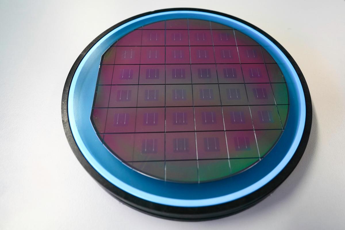
This builds on a 2017 demonstration from Graphenea and AMO of graphene photodetectors with bandwidth exceeding 75GHz, fabricated on a six-inch wafer process line. Modulators and photodetectors are the two main component types currently attracting interest, according to Zurutuza. ‘But non-linear optical switches, lasers, saturable absorbers, it has potential in all those devices,’ she observed. ‘Photodetectors are probably closer to market than other components, but in all of them, graphene makes sense. Also, currently the modulator and photodetector are manufactured separately and assembled in the chip, while with graphene everything will be fabricated at the same time on the chip.’
The market for modulators and photodetectors will be similar, Zurutuza suggests. For commercialisation of modulators and photodetectors in telecommunications, 12-inch wafers will be required and ‘the larger the wafer, the more complicated things become’, she said. She stresses that this will slow down the time to market, so graphene products in other applications are nearer realisation. ‘The requirements in optical communications are maybe stricter,’ Zurutuza said. ‘You need very high charge carrier mobility, and it’s also going to take longer to do it at a larger scale.’
Ahead of the curve
Looking more broadly, graphene promises features that can’t be realised with conventional technologies, Templ stressed. ‘A 1:1 application of conventional device- and system-concepts bears the risk that we miss a number of interesting options,’ he said. ‘The hierarchy and structure of the networks requires combining and extracting data traffic to/from segments with higher bundled traffic and distribute by means of ramified network segments with lower traffic down to the individual users and homes. New-material-based components can’t change that. But said components can significantly change how we utilise and exploit such networks by improving on the dynamics, flexibility, performance and efficiency.’
Meanwhile, applying graphene to wellestablished device concepts could unleash features beyond the high charge carrier mobility that supports extremely high bandwidths and bitrates. In particular, graphene-based plasmonic optical modulators and detectors might open the way to highly integrated devices enabling communication with bitrates of several Tb/s. Such networks could enable a ‘deep communication experience of entirely different quality to what we have today,’ Templ said.
D’Errico is similarly excited by graphene’s prospects, but recognises the challenges faced in delivering them. ‘Since I started with graphene, every successive step was more brilliant than the previous one,’ he said. ‘At every step, we answer some questions – but we also ask an enormous amount of new questions.
Andy Extance is a freelance science writer based in Exeter, UK