There are many challenges to overcome to provide quick and efficient characterisation of photonic integrated circuits, finds Andy Extance
Today the internet is the fastest it has ever been – but that achievement brings enormous optical communication testing challenges. That’s underlined by Jeroen Duis, chief commercial officer of Phix Photonics Assembly in Enschede, Netherlands, which performs hybrid integration of chips, assembling multiple chips into a single package. ‘Customers would like to have a transmission test to validate that the whole module is working correctly,’ he explained, adding that test systems cost hundreds of thousands, or millions, of dollars. That value disappears in two or three years as communication speeds accelerate, Duis said.
These tests should reveal the number of bit errors, resulting in signals producing false zeroes or ones in the digital domain. But low error rates and the greater functionality of transceivers have lengthened testing, requiring more time to collect sufficient error data. ‘Typically, the testing is four to eight minutes per product in a volume environment,’ Duis explained. Consequently, when manufacturing scales up, expensive but short-lived test systems ‘need to be duplicated and operated in parallel,’ he added, creating regular significant expenses.
Such challenges intensify with photonic integrated circuits (PICs), currently made in fairly small volumes. Yet these are the same devices delivering vital technical advances. Therefore, PICs must be made on a larger scale. Contract manufacturing companies such as Phix, equipment makers, universities and industry groups are therefore coming together to develop test and measurement technology and standards to enable that.
Step-by-step
Testing could be done at various steps of manufacturing, Duis explained, including analysing deposition and etching to achieve full statistical process control at the wafer level. ‘However, this works only in continuous highvolume manufacturing,’ he said. ‘Most photonic chips are made in batches with small quantities.’ Typically, the first optical tests are only done after fabricating PICs, when semiconductor wafers have been diced to form chips. A first verification step reveals whether a design and/ or process can meet expectations. If the chip fails it must be excluded, whether the problem is with chip design or the manufacturing process. ‘After the issue is found, one needs to correct for this, and start a rerun, which easily pushes delivery back four months,’ Duis said.
Sylwester Latkowski, from the Photonic Integration Technology Centre, at Eindhoven University of Technology (TU/e) in the Netherlands, notes that things can be simpler once verification is complete. ‘It is, in general, cheaper if we can detect known-good-die (KGD) as early as possible in the production chain,’ he said. ‘Only then can we take adequate countermeasures to optimise cost of production.’ Validating dies to prevent faulty ones entering the supply chain cuts costs and frees up capacity. If some chips can’t deliver at full expected specification, they could perhaps be repurposed, Latkowski added. Wafers might also be discarded before dicing, if testing shows that too many chips would be rejected.
Working together
Latkowski and his colleagues are working towards standardising and automating test methods to enable this early validation. For example, TU/e runs the Open Innovation Photonic ICs (OpenPICs), InPulse and OIP4NWE pilot-lines, which are seeking to develop an industrial platform for PICs. He is also working with the PIXAPP PIC assembly and packaging pilot line, led by the Tyndall Institute in Cork, Ireland. ‘We are starting with small steps, trying to unify chip layouts and implementing test methodology at the design level,’ Latkowski said. ‘These allow designers to work on the application-specific photonic integrated circuits, while taking into account testing and also assembly aspects. It also benefits automated test equipment vendors, by helping them to develop modular tools. Such modularity will lead to scalable solutions that will allow for a certain degree of customisation with a minimum cost related to non-recurring engineering.’
But combining electrical and optical testing is especially challenging, Duis noted. He emphasised that there can be more than 100 critical parameters to test. This is difficult in ‘low-volume, high-mix prototypes with different contacting configurations’, he added. ‘Foundries need a minimum amount of runs through the fab with the same design, such that they can build up knowledge on how customer-specific critical parameters behave on a PIC level,’ he said.
Foundries and their customers can work together to optimise PIC designs for testing. For example, they could exploit selfdiagnostics, so the foundry can run purely electrical tests on a standard wafer prober. If not, they need to couple in light, using active alignment with fibre-probers on a wafer or chip level. Agreeing this might take years, Duis warned. ‘In order to speed up this process, foundries must have better statistical process information on all the offered building blocks, reducing the amount of critical test parameters that need to be tested,’ he said.
Complex proposition
FiconTEC is involved with many such projects, explained Gregory Flinn, marketing development spokesperson for the firm, which offers automated stand-alone and in-line photonics assembly and testing systems. The latter can validate or verify photonic chip or device performance at any process stage, to check that electrical and optical characteristics are within the specifications.
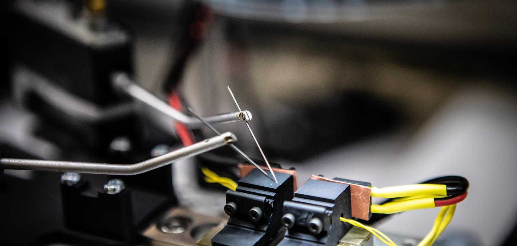
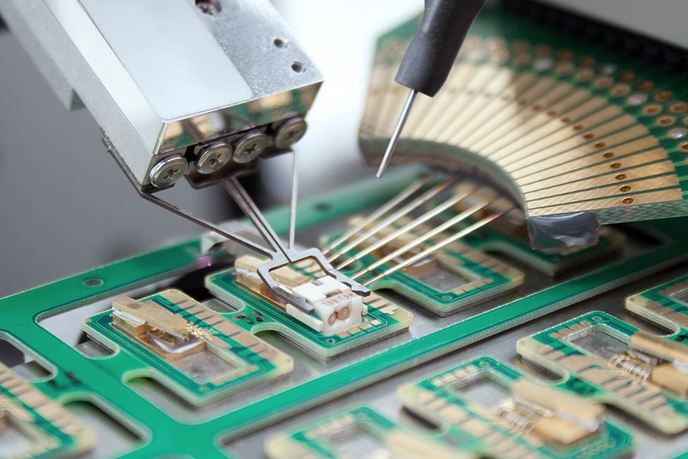
He explained that in these systems, ficonTEC provides high-resolution mechatronic positioning systems that align pickups to devices or wafers, enabling the connection to test equipment. Yet adequate, dedicated electro-optical probe heads are lacking, he said. That’s partly because they are a much more complex proposition than electrical testing probe heads alone, which themselves can have many tens of thousands of pickups.
‘Electrical pickups require only metal contacts, each one comprising a pad that is around 80µm by 80µm,’ Flinn said. ‘Our assembly machines integrate PIC devices together with other micro-optical photonic components to assemble a complete photonic device. That device then needs to be tested, and you may be testing for multiple characteristics.
ʻIf the plan is to use electro-optical mixed-signal pickups, then your resolution bounds are entirely defined by the optical side, which can be down to 20nm. In general, the actual alignment takes more time, and places much greater demands on the positioning system, which also means it’s more costly from a capital outlay aspect.’
Time for a compromise
To qualify precision in optical fibre alignment to on-wafer devices, ficonTEC has developed and demonstrated systems. For example, one system went to the University of Southampton’s Optoelectronic Research Centre’s Silicon Photonics Group. The system is intended to have many additional capabilities, said Flinn.
A similar demonstration system appeared at NI Week in Austin, Texas, in May, and at Laser World of Photonics, in June. It aligned dual fibre arrays to couple multiple light signals through multiple on-wafer waveguides. For this purpose, ficonTEC teamed up with optical communication test and measurement equipment supplier Coherent Solutions. In the demo, Coherent Solutions provided the necessary optical input/output test instrumentation to illustrate coupling through the waveguides.
Hansjoerg Haisch, program manager, networks and data centres at Keysight Technologies, agreed that fast, high-precision alignment is needed. However, he also highlighted several other challenges. ‘Coupling light into waveguides through widely-used grating couplers depends strongly on light polarisation and wavelength,’ he stressed. ‘Stability of polarisation state, or good knowledge of the state of polarisation, is essential for repeatable and low uncertainty measurements.’ Haisch adds that coupling light into waveguides through the device edge is not usually possible before dicing wafers without using test structures. However, coupling to the edge through etched trenches has recently been developed.
Making a compromise
Furthermore, PIC wafers or lone chips cannot always be operated under realistic conditions, as they often require amplifiers or lack the heat sinks that will let them run at high power. ‘On-wafer PIC test coverage is thus generally restricted to a few parameters and later module or finished good performance must be predicted based on those few measurements,’ Haisch said. ‘For highly complex PICs, not all functions can be interfaced or accessed independently, without integrating too many monitoring functions, which would need too much chip real-estate. A compromise between test coverage and test time must be found for known good die selection and throughput.’
Reaching higher production volumes helps make testing equipment more economical, explains Haisch. ‘PIC customers have been reporting increasing volume shipment of PIC-related technology for their datacom products in the last two years,’ he added. Keysight has helped by partnering with PIC industry players to standardise photonic parametric tests. This involves migrating Keysight’s years of test and measurement experience and expertise from the optical transceiver market.
Keysight’s current photonic test and measurement products are at least 10 times faster and more accurate than its first designs, with ‘hundreds of patented new technologies’, Haisch added. ‘As complexity of PIC design and implementation varies, some only work on passive structures, while others bring in ring resonators and even lasers,’ he said. ‘The test and measurement requirements also vary, and we have been supporting each individual requirement from each foundry and intellectual property designer.’
Self-testing on the roadmap?
To clearly define the interface between device and test setup, Keysight has introduced calibration and de-embedding methods Haisch noted. This removes the test setup’s impact on a device’s characteristics. ‘Keysight’s photonic applications software suite speeds and simplifies both the process of test setup and the optical measurements,’ Haisch said. Keysight also partners with probe station vendors like Formfactor. Such relationships help integrate probe stations with optical, electrical and radio-frequency probes, and cards with test instruments in an overall test solution, Haisch said. Finally, Keysight Pathwave Automation provides a platform to define and realise test flows and communicate with test instruments, probe stations and databases. This overall solution was demonstrated live at the OFC conference in March.
Approaches that test PICs through external interfaces can be complemented by selftesting functions, Haisch added. ‘Designers work on incorporating self-test features onto PICs, to check functional operation, rather than performance,’ he said. Approaches include optical loopback between transmitter and receiver, or optical monitors tapping off signals. ‘Since electronics are not, and potentially will never be, monolithically integrated with PICs – maybe with the exception of very simple electronic functions – self-testing is for testing at module level, rather than wafer-level testing,’ he said. Haisch added that this is due to greatly differing semiconductor technology for high speed electronics, which uses 7nm-scale lithography, and silicon photonics, which uses 90-130nm lithography.
In tune
However, Latkowski is more optimistic about electronic-photonic integration, and outlined some self-testing options that might be possible. ‘Initially PICs could, for example, monitor basic properties such as temperature, output power or wavelength of a laser.’ He hoped that it would be possible to implement relatively simple feedback circuitry that could then take corrective action. For example, it could increase current injection into a laser, should it face a drop in output power. Alternatively, the circuitry could cut off the current injection should the chip overheat. Another option would be to tune a laser should its wavelength be drifting.
‘Next to that, if we could implement advanced logic – for which even more support from digital electronics may be needed – PICs could monitor a wide range of parameters, and adequately react to those,’ said Latkowski. Options include recalibrating laser arrays or switching between high-performance or energy-saving modes, like systems-on-chips in smartphones, Latkowski highlighted. ‘This should be possible for PICs, when intimate electronic-photonic integration matures,’ and is on the Integrated Photonic Systems Roadmap. In the meantime, Latkowski highlighted that standardisation efforts must become widely recognised as successful. And if they are, they will first benefit prototyping, multi-project wafer (MPW) foundries and other low-volume production scenarios.
‘For large volumes, at a certain threshold there will always be a need for customisation in order to optimise the cost,’ Latkowski said. But the two do not conflict, he observed. ‘Standards, even if used in small prototyping batches, should be defined in a way that supports scaling to volume.’ That’s because test and measurement equipment suppliers, PIC foundries, assembly and packaging service providers all want the same thing, Latkowski said. ‘We are all looking for a “killer application” that will drive the volumes.’
Andy Extance is a freelance science writer based in Exeter, UK