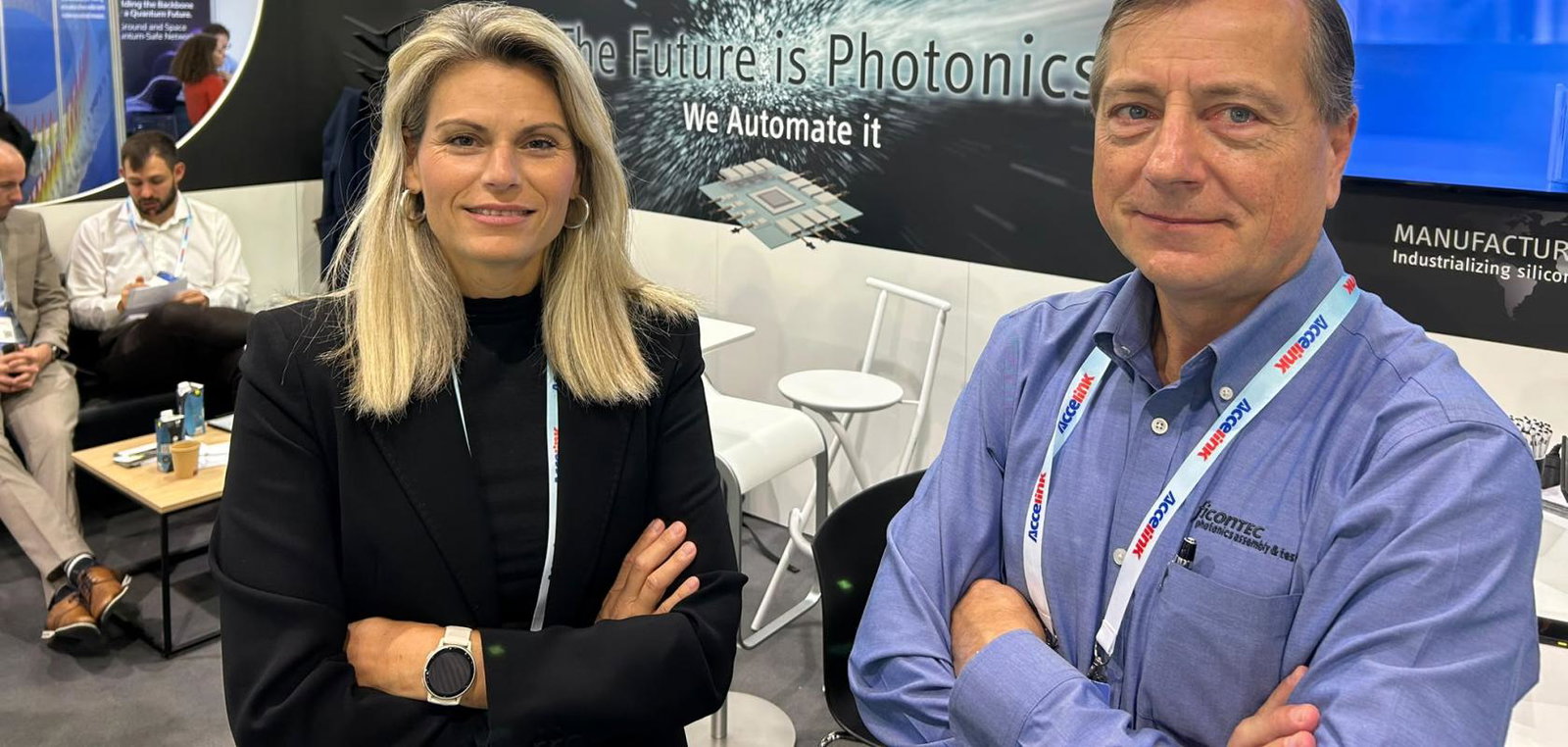
With increased demand across the semiconductor and photonics industries for scalable assembly and testing solutions, ficonTEC used ECOC 2026 to leverage its 25 years of expertise to evolve from a largely custom-build supplier into one that can deliver machines at scale.
Its booth theme, ‘The future is photonics – we automate it’, sought to illustrate the company’s readiness to support the widespread adoption of photonic devices in the vibrant markets of AI infrastructure and next-generation communications. Stefano Concezzi, Chief Marketing Officer, told us: “The real challenge is manufacturing photonic devices reliably, repeatably and at the volumes the market will require.”
At its booth, ficonTEC demonstrated both how it delivers against this challenge and how it supports the transition to intelligent automation across the photonics manufacturing chain – from fibre preparation and high-precision assembly to testing at wafer, die and module level. “The message we want visitors to take away is that scaling photonics is not simply about increasing production speed,” said Concezzi. “It requires stable processes, high-precision alignment, effective testing, improved yield and close collaboration across the entire ecosystem.”
The company’s main focus at ECOC 2026 was to demonstrate its capability to provide scalable manufacturing solutions for emerging applications such as silicon photonics, co-packaged optics, optical I/O and next-generation transceivers. The ability to now provide these machines at scale – while still offering a degree of customisation at the configuration stage – puts the firm in a position to supply key markets such as global chip manufacturers, PIC foundries and OSATs (outsourced assembly and test). Scalable electronics assembly is well established, but the need for scale is relatively new for photonics assembly.
“A particularly important area for us is automated electro-optical testing,” said Concezzi. “Through our dedicated ficonTEST business unit, we support customers with testing solutions at wafer, die and module level. This includes single- and double-sided testing concepts designed to identify performance issues earlier in the manufacturing process and provide reliable data before expensive devices are integrated into complete modules or advanced packages.”
ficonTEC also highlighted its capabilities in high-precision automated assembly and active alignment, as well as automated fibre preparation and attachment. These processes are essential for achieving the repeatability, throughput and yield required for volume manufacturing.
“What differentiates our approach is that we do not look at assembly, fibre preparation and testing as isolated steps,” explained Concezzi. “We combine process expertise, automation and flexible system architectures to help customers establish a scalable manufacturing process – from initial process development through to high-volume production. This is the foundation of ficonTEC’s Lab-to-Fab approach, which shortens the engineering V-model timeline by enabling customers to move seamlessly from design and process development through validation and into high-volume manufacturing, while leveraging common software and hardware architectures across the machines used at each stage.”
In a competitive field, ficonTEC is keen to point out its breadth of expertise across the photonics manufacturing chain. “We are the only company bringing together automated fibre preparation, precision assembly, active alignment and electro-optical testing within one organisation,” says Concezzi. “It takes a unique blend of technologies and competences to deliver what we do.
“However, our differentiation is not only technological. We work closely with customers from the earliest stages of process development, helping them transform a technically viable concept into a stable and scalable production process. Our systems are modular and configurable, allowing us to respond to different product designs, maturity levels and production requirements.
“We also have extensive experience in some of the most demanding photonics applications, where sub-micron precision, process stability and traceability are essential. This combination of application knowledge, process expertise and production automation allows us to act as a long-term manufacturing partner rather than simply an equipment supplier.”
Concezzi is keen to emphasise that scaling photonics can only be achieved through collaboration throughout the ecosystem. “No single company can solve all the challenges involved in moving silicon photonics and advanced optical packaging into volume production,” he said. “Device designers, foundries, material and component suppliers, packaging specialists, equipment manufacturers and test experts must work together much earlier in the development process.”
Indeed, the company demonstrated this approach in practice by hosting an expert seminar alongside ECOC 2026, bringing together representatives from across the European photonics supply chain to discuss what it will take to move from innovation to industrial-scale manufacturing. “ECOC was therefore not only an opportunity to present our technology,” concluded Concezzi, “but also an opportunity to engage with the ecosystem, understand the industry’s next manufacturing bottlenecks and explore how we can address them together.”
For further information, please visit www.ficontec.com.