By any conventional measure, Photonics West is an overwhelming event. The world’s largest photonics exhibition sprawls across materials science, optical communications, sensing, free-space optics, and emerging quantum technologies. For VIAVI Solutions, however, that breadth is precisely the point.
“Photonics West is an interesting experience for us because it’s such a broad show that goes madly off in all directions,” says Matthew Adams, Director of Product Management for Fiber Optic Production and Lab Test Network & Service Enablement at VIAVI Solutions. “But that’s exactly why it has become so important to us.”
A decade ago, the optical communications side of the photonics industry had largely consolidated around specialist events such as OFC and ECOC. Product roadmaps narrowed, customer sets stabilised, and innovation followed predictable tracks driven by vertically integrated telecom operators. Photonics West, by contrast, felt unfocused – rich in ideas, but perhaps distant from deployment realities. That changed as the centre of gravity in optical communications began to shift.
“As the dominant use case moved away from telco verticals and towards hyperscalers – and now AI hyperscalers – the assumptions that underpinned the ecosystem started to break down,” Adams explains. “Suddenly, there was a hunger for new approaches, new technologies, and Photonics West came back into relevance because it’s such a strong ‘ecosystem’ show.”
AI data centre and AI compute factory build-out test and measurement
Today, the event has become a strategic show for VIAVI. The reason lies not only in what is being built, but in how fundamentally the rules of photonic scale are changing.
Optical communication, which is morphing into AI data centre and AI compute factory build-out test and measurement, is a key focus area for VIAVI. Another focus area is its material science businesses – filters, coatings, and now expanding into sensing.
VIAVI brings decades of leadership in photonics. That lineage stretches back to JDSU, a name synonymous with photonic innovation for decades. “People don’t always recognise just how much photonics is in the company,” he says. “We have five different physical sites globally involved in photonics. There’s a real storehouse of technology, and we’ve continued to evolve it.”
VIAVI has expanded its portfolio for global networks, moving upstream and augmenting its installation, commissioning and maintenance tools with solutions for lab, production and manufacturing.
“The role of the lab and manufacturing – scaling fabrication technologies – is now central,” Adams says. “We’ve transformed into a technology leader driving fabrication and manufacturing enablement.”
That transformation is being accelerated by AI infrastructure at a pace the industry has never experienced.
When data rates stop replacing each other
The industry narrative around optical evolution has long been dominated by clean generational shifts: 10G to 100G, 100G to 400G, and so on. Adams argues that model no longer applies. “We’re coming out of an era where technologies replaced other technologies,” he says. “Now, they layer.”
In AI data centres, multiple data rates coexist by necessity. “There are places where 400G still makes sense, where 800G makes sense, and where 1.6T makes sense. And that makes everyone’s life more complicated,” he says.
Even the headline speeds themselves mask deeper complexity. “When people say ‘1.6 terabit’, there are actually about six different versions of that,” Adams notes. “Is it coherent? Is it parallel optics DR? Each choice completely changes the photonic ecosystem you’re part of – and what you need to test and manufacture.” At the same time, the luxury of gradual ramp-ups has disappeared. “There used to be a training-wheels phase. You’d ship a first version, learn, then make your money on the second,” he says. “That’s gone. You’re either right from day one, or you miss it. That’s what makes this such a high-stakes environment.”
Fibre-wide thinking flips the economics
Perhaps the most profound shift Adams describes is what he calls the move to “fibre-wide” architectures. “In long-haul and metro networks, fibre was precious,” he says. “The goal was to squeeze as much bandwidth as possible out of every fibre pair.”
AI factories invert that logic. “I need to go 10 metres, 50 metres, maybe 500 metres. Fibre is effectively free compared to everything else. So instead of fibre pairs, I can deploy thousands of fibres.”
That change rewrites the constraints of system design. The limiting factor is no longer the physical infrastructure, but the interface between fibre and silicon. “The real bottleneck becomes edge bandwidth – how much data you can actually get into the chip,” Adams explains. “And that’s why silicon photonics has gone from niche to essential. You simply can’t scale thousands of channels with discrete components.” Once that decision is made, everything follows: co-packaged optics, new connectivity models, and radically different installation practices. Fibre connectivity inside data centres is changing so fast, it can be hard to keep up.
For suppliers, this environment demands a new way of engaging with customers. “The velocity of these discussions has never been higher,” Adams says. “They often start very prescriptive – customers want standardisation because the scale of the problem is so new.”
But that rigidity is fragile. “Six months later, if they decide there’s a better way, they’ll change direction on a dime. Time and even sunk cost aren’t the primary concern,” he says. That forces suppliers to balance responsiveness with innovation. “You have to listen carefully, but you also have to bring your own ideas. You can’t assume anything is chiselled in stone. If you can show a better way, customers are extremely receptive.”
As AI data centres scale, the challenge is no longer conceptual – it is brutally physical. “We talk about building these enormous data centre buildings,” Adams says. “But then you have to fill them. And, behind that, there’s another cascade of manufacturing facilities that also need to scale.”
The problem is speed. “They want to build AI factories faster than we can build manufacturing space,” he explains. “These aren’t simple warehouses – they’re cleanrooms, which are highly specialised facilities.”
That reality has elevated factors that once seemed trivial. “Physical density now matters. If I can get four times the output in the same manufacturing footprint, that’s transformative. Ten years ago, nobody cared about the physical density of manufacturing test equipment. Now it’s a major driver.”
A gold rush – but not like 2000…
The frenetic pace has prompted inevitable comparisons to previous industry booms. Adams sees similarities, but also crucial differences. “It has elements of a gold rush – the energy, the urgency,” he says. “But it’s very different from 2000.”
The difference, he argues, is maturity. “There’s a much deeper solution space and a far more mature supply chain. Back then, everyone needed the same pick and shovel. Today, there are multiple viable ways to solve the problem.” That diversity provides resilience, even under strain. “I don’t have a dozen ways to solve everything, but I usually have two or three. That gives the industry room to adjust.”
Supply chain pressure remains intense, but VIAVI’s approach offers insulation. “We fabricate our own optics for metrology platforms,” Adams explains. “We’re not competing with hyperscalers for commodity components.”
That vertical integration matters when volumes diverge dramatically. “If you’re trying to buy the same component a hyperscaler is buying a million of, and you only need a hundred, you’re at the bottom of the list,” he says. “By going deeper – lenses, prisms, coatings – we maintain flexibility.”
Looking ahead, Adams identifies three priorities. The first is immediate and operational.
“We have to match or exceed our customers’ manufacturing ramps,” he says. “That’s priority number one.”
The second is strategic discipline. “Everyone’s shipping product right now, but customers are already saying, ‘We don’t want to do it this way forever.’ We need to keep investing in next-generation processes even while volumes are high.”
The third is timing. “Our customers know they’re running out of power and space. That narrows their options. Our job is to be ready – not just with the right technology, but at the right moment.”
A layered future
Are today’s AI data centres future-proof? Adams is candid. ” I don’t think things are settled,” he says. “We’re in a washing-machine cycle right now.”
Photonics, he notes, evolves differently from digital technologies. “Every five years, we harness a new piece of physics, but it sits on top of what came before. We don’t throw anything away – we just keep adding layers!”
That layered evolution, combined with a still-collegiate culture, remains one of the industry’s defining strengths. “It’s a multi-hundred-billion-dollar industry, but we’re still discovering things we didn’t know,” Adams says. “And people genuinely celebrate each other’s breakthroughs. That’s a huge asset.”
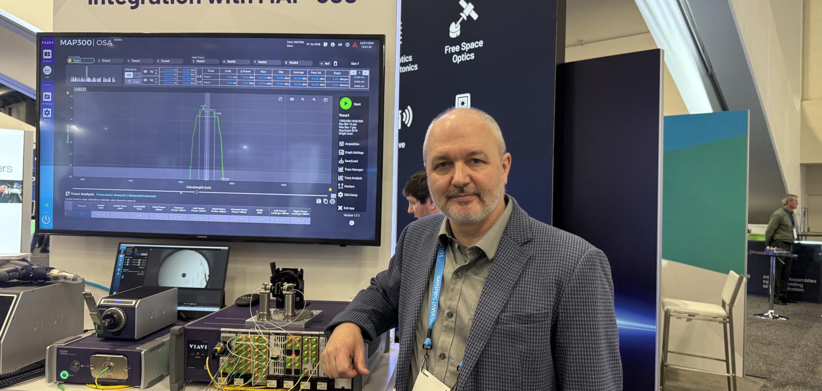
Photonics West is also an opportunity to show off products, of course. As AI data centres and so-called ‘AI factories’ drive unprecedented scale in photonic manufacturing, flexibility in test and measurement has become as critical as raw performance. VIAVI Solutions’ MAP-300 metrology platform, showcased at the San Francisco event, has been developed to meet that challenge, offering a modular approach designed for an increasingly complex communications ecosystem.
“The MAP-300 is the metrology platform,” explained Adams. “There are about 25 different metrology modules that customers can mix and match and build out.” That modularity is key as data rates and physical interfaces proliferate. Whether the requirement is ER, DR, FR or LR, Adams notes that the real challenge is precision alignment between interface, data rate and manufacturing process. “What you’re really saying is, ‘I want to build something that exactly matches the requirement of the data rate and exactly matches the physical interface.’ And these platforms can do all of that.”
By reconfiguring module combinations, the MAP-300 can address approximately 90% of the communications photonics ecosystem, spanning silicon photonics integration, module assembly and system-level testing. VIAVI deliberately focuses on this “middle space” of the value chain. “We’re not working at the raw material level,” Adams said. “We’re integrating silicon photonic chips, packaging them, building modules, and integrating into systems.”
Crucially, the MAP-300 also anchors a broader manufacturing workflow. As fibre-wide architectures drive millions of fibre and connector terminations, Adams highlights that inspection and cleaning have become the primary bottlenecks to scale. VIAVI’s complementary inspection and non-contact, vapour-based cleaning solutions provide what customers have “been begging us for – an on-ramp,” ensuring connectors are clean before being connected to high-value metrology systems.
Together, the MAP-300 and its associated inspection and cleaning tools reflect a shift in broader photonic manufacturing priorities: from isolated test steps to fully optimised, scalable process flows capable of keeping pace with AI-driven infrastructure growth. It’s an ecosystem VIAVI is capable and confident of commanding.